partners
Partnering with Innovators
ACCURACY is committed to building an open industry ecosystem — together.

.png)
.png)

.png)
.png)





.png)


.png)
.png)
.png)
.png)

.jpg)
Driving Industry Innovation
ACCURACY, founded in 2010 in Suzhou, specializes in high-precision, intelligent micro-assembly and die-sorting equipment with 50%+ R&D staff.
The product portfolio includes multi-chip die bonder, sub-micron high-precision die bonder, intelligent sorting systems, and more — widely applied in advanced packaging, IC packaging, power semiconductors, optoelectronics, sensors, and related fields. The company is committed to delivering comprehensive die attach solutions from process development to mass production deployment.
Comprehensive quality management system
Continuous investment in core equipment R&D
Covering Global Industry Clusters
Joint R&D with Top-Tier Universities
ACCURACY is committed to building an open industry ecosystem — together.
From R&D to mass production — full coverage for diverse production needs
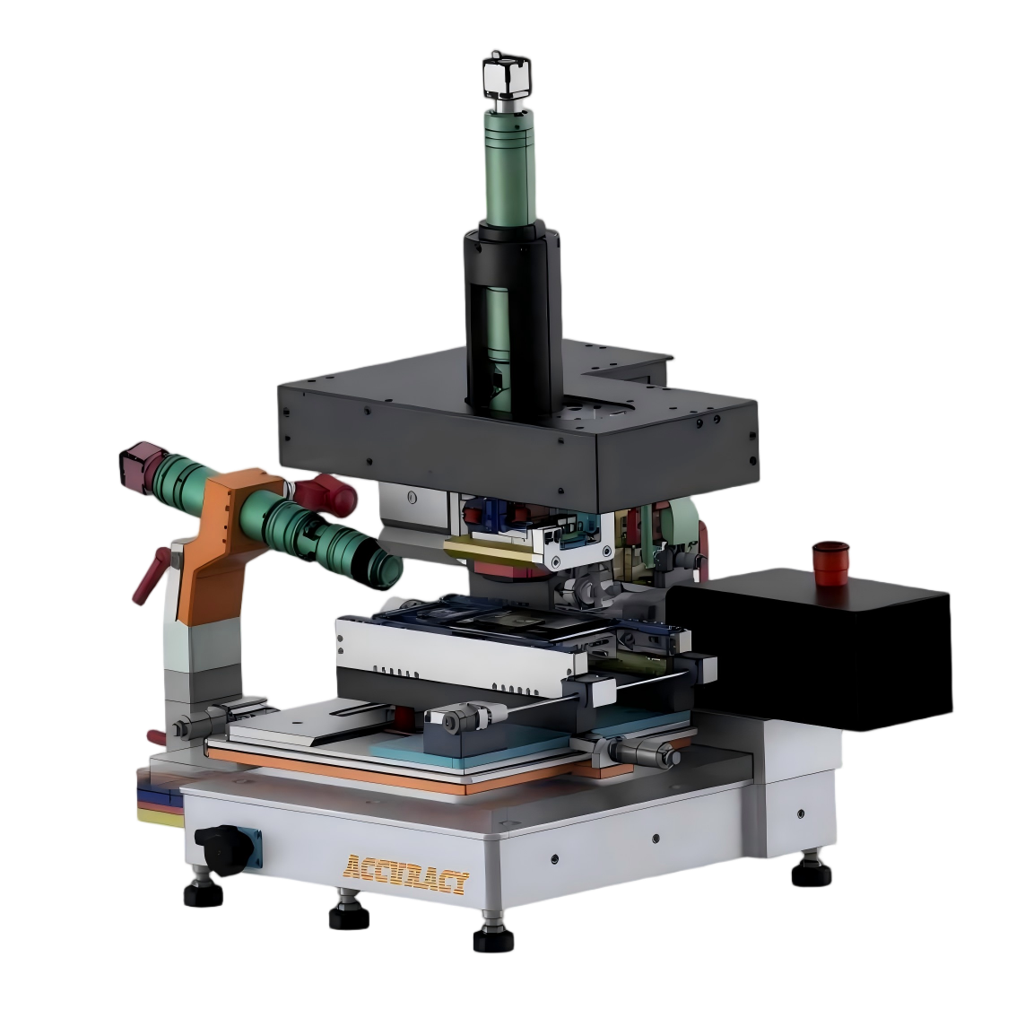
Standard-die placement accuracy: ±0.5μm Force: 0.1 N–30 N Temperature: 450°C ± 1°C
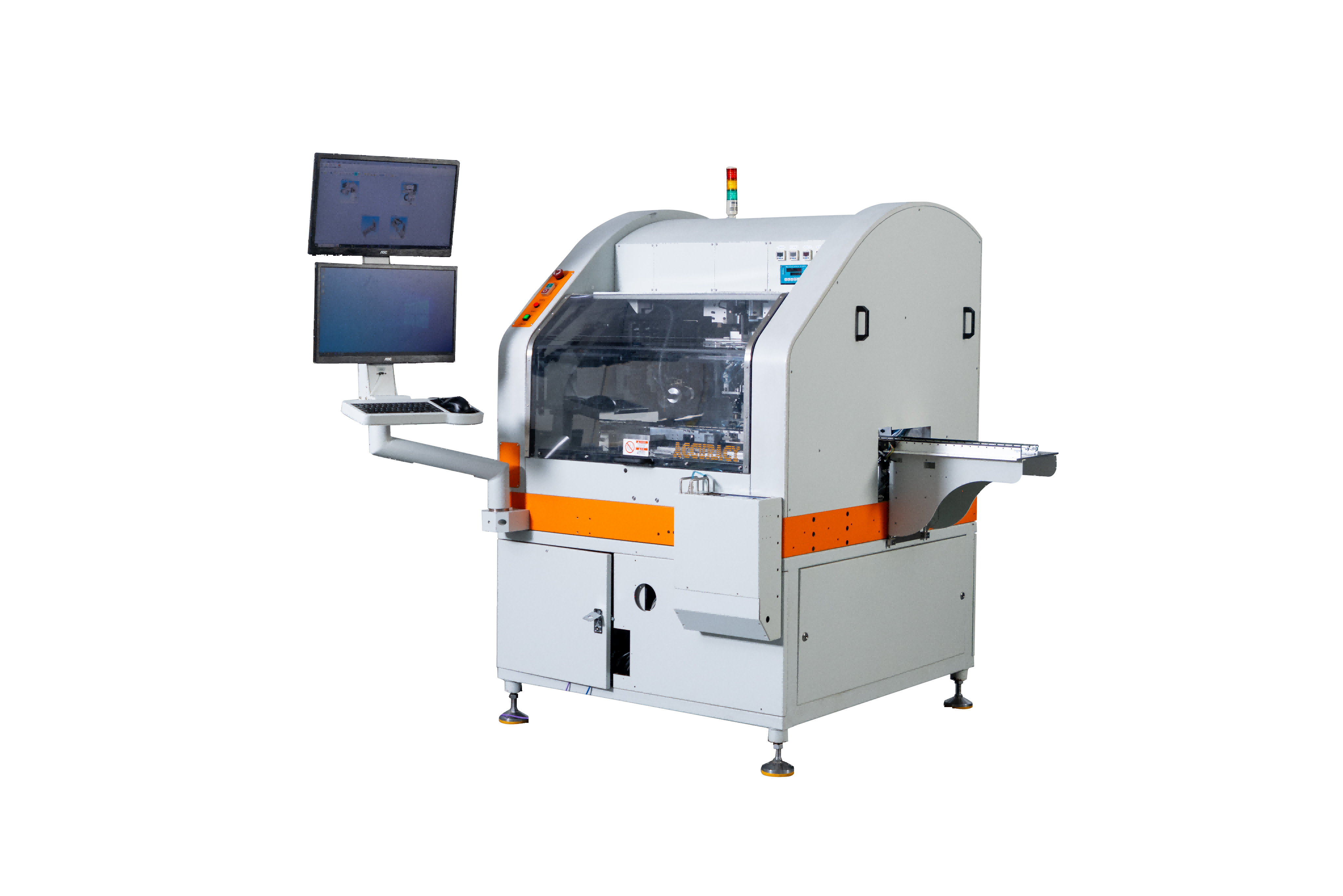
Placement Accuracy: ±3/7/10μm Supported Process: Epoxy / Multi-Chip / Flip Chip / DAF
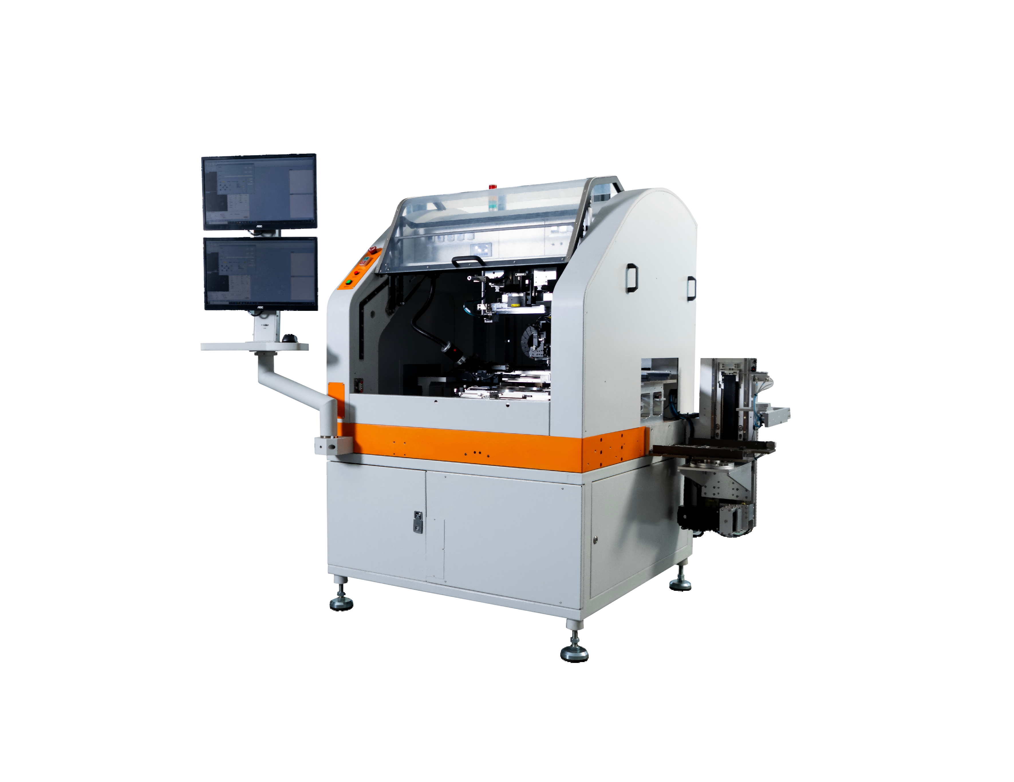
Placement Accuracy: ±10/25μm Sort Modes: Film/Tray to Film/Tray
Placement Accuracy: ±38μm Sorting Modes: Film/Tray to Film/Tray
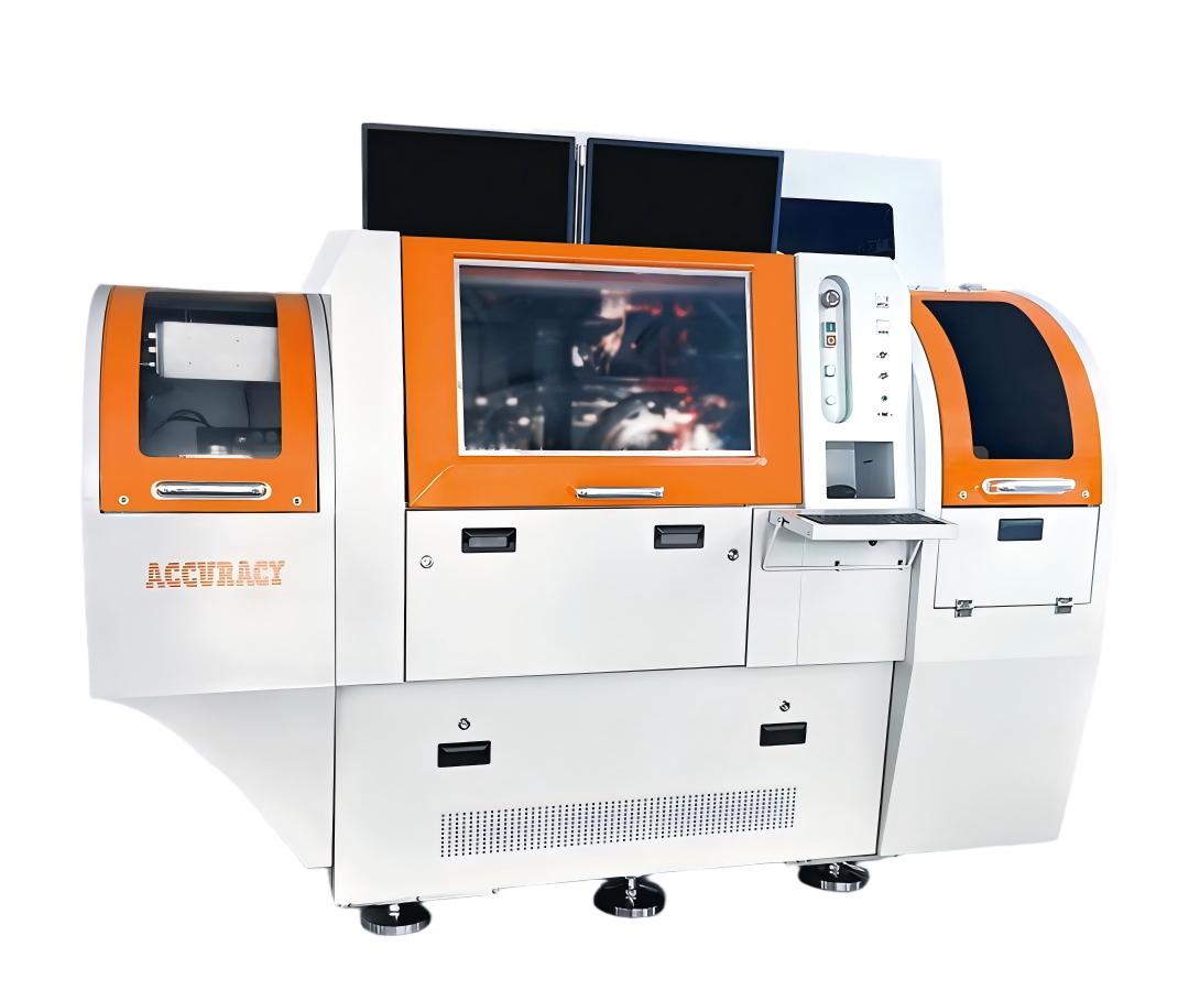
Placement Accuracy: ±25μm Supported Wafer Size: Max 12"
Full-cycle R&D and engineering deployment capabilities.
Covers full-scene mounting needs from traditional packaging to advanced packaging
High-precision die bonding solutions for traditional packaging processes: QFP / BGA / LGA / QFN
Advanced packaging and precision die bonding for high-performance computing chips: GPU / NPU / HBM
Micro-assembly and hermetic packaging for MEMS devices: IMU, pressure sensors, micromirrors and more
AuSn eutectic bonding and high-reliability die attach for RF/microwave devices: MMIC / PA / LNA
High-precision alignment and micro-assembly for photonic devices: VCSEL / LiDAR / silicon photonics, meeting optical communication and sensing demands
Complete die bonding solutions for advanced packaging processes: Interposer / 3D Stacking / Fan-out
From Micro‑assembly to Packaging — Sub‑micron Precision
Began independent R&D of semiconductor packaging equipment.
In 2015, the first-generation IC die bonder entered Huatian's supply chain, making it one of the early domestic equipment vendors to localize this process.
Launched Fan-out high-precision die bonder; over 200 units deployed.
Per the China 3D IC Alliance public directory, became a member back-end bonder maker in the alliance.
Undertook Jiangsu Core Technology R&D Project.
Accuracy surpassed 500nm; per Yole Group 2025 report, became the first Chinese C2W supplier featured in its reports.
For product inquiries, technical support, or partnership opportunities — reach out anytime.