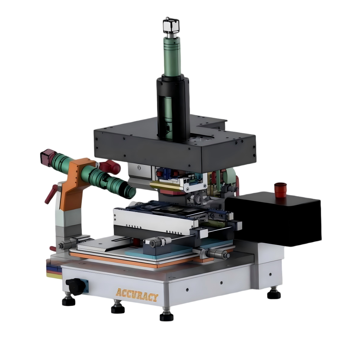
Die Sorting Multi-Function Sorting Expert
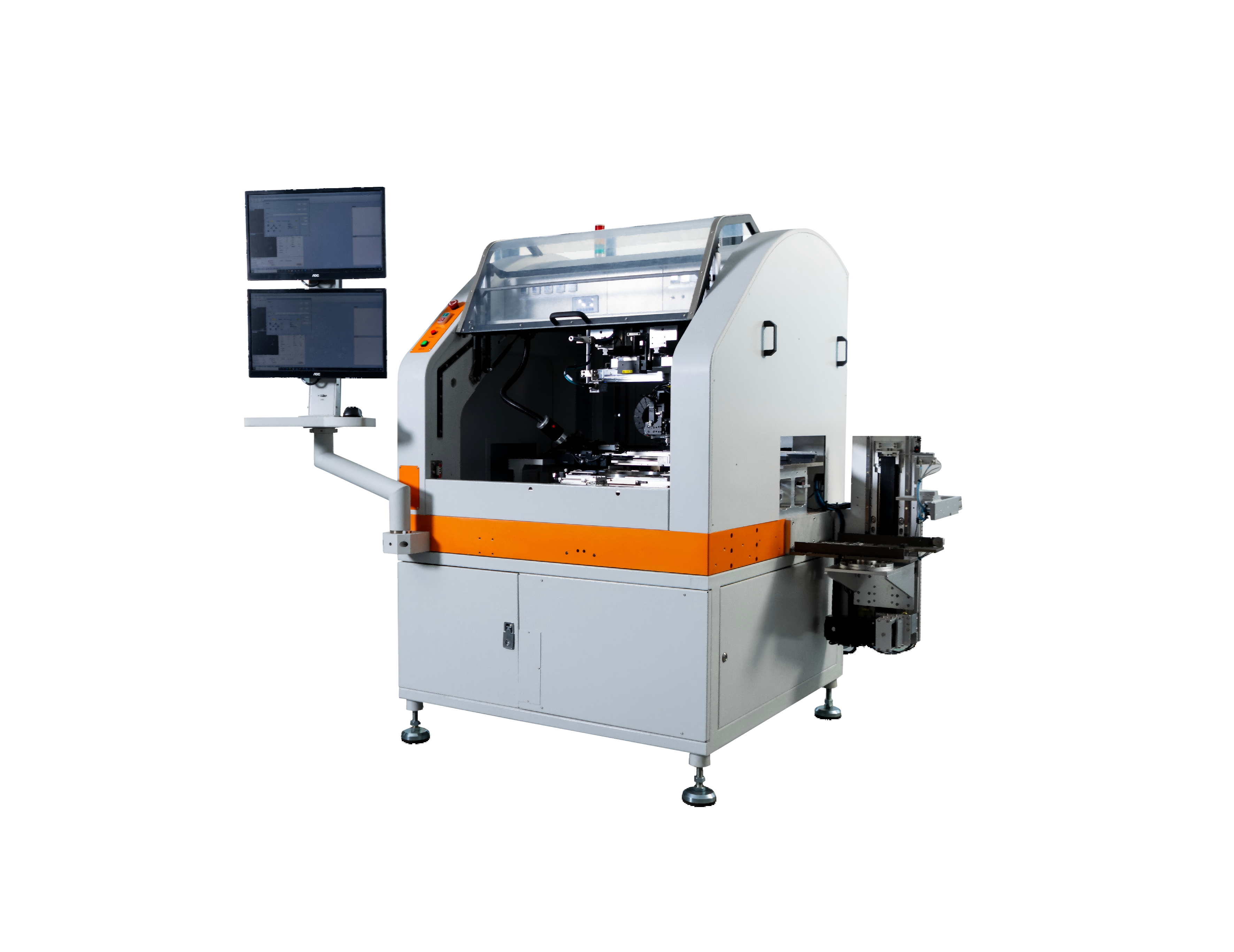
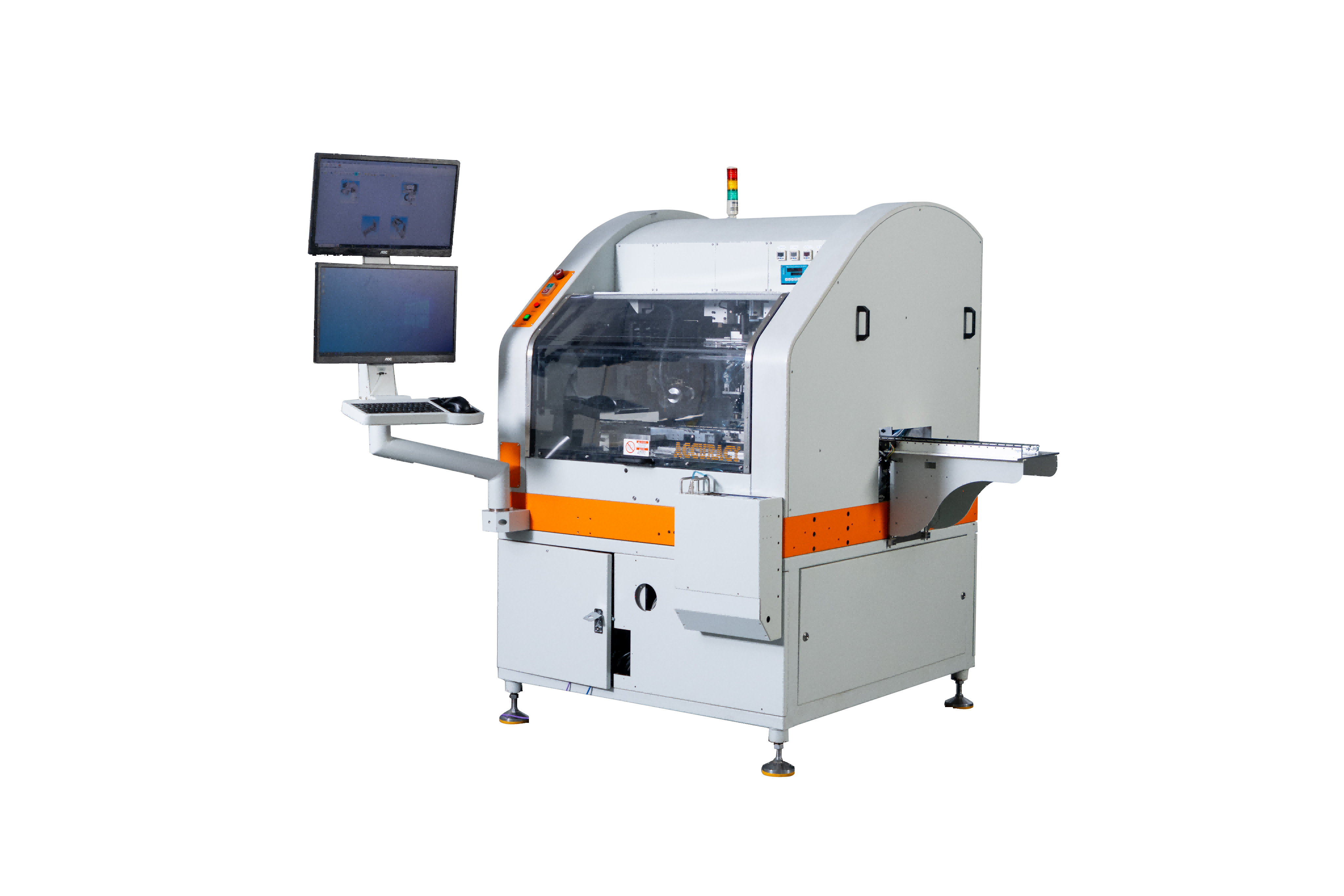
RX2000SP3
8" Multi-Function Die Sorter

RX2000 SP3

±38μm ·8" Wafer

±38μm
Placement Accuracy
Max 4K
Throughput (UPH)
Max 8"
Wafer Size

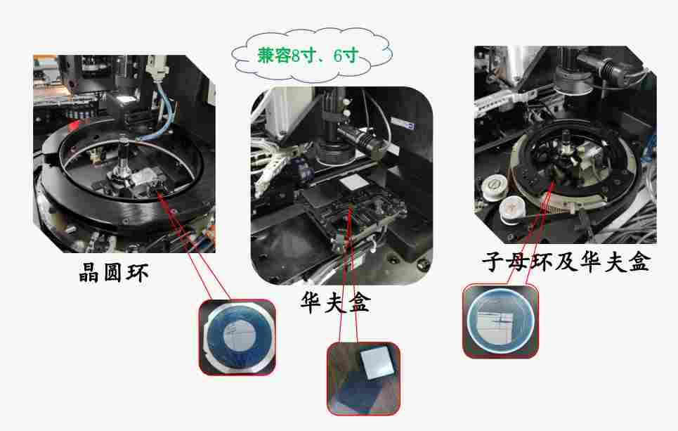
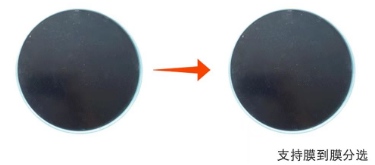
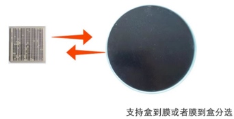
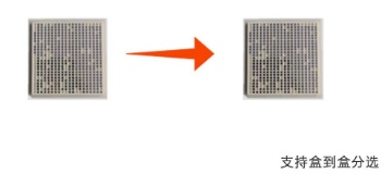
The RX2000SP3 supports film-to-film, tray-to-tray, tray-to-film, and film-to-tray sorting modes. It handles panel wafers, multi-bin wafer map sorting, and adapts to diverse production requirements.

Application Cases

RX2000 series: 100+ systems shipped, 10+ years production-proven, serving 30+ customers

Silicon Photonics / VCSEL Die Sorting — Optical Communications Manufacturer
Application Cases
Optical Transceiver Dies

Optical Transceiver Dies

Silicon photonics, VCSEL/PD chips, and optical components sorting. Supports ultra-thin die pick-up, special structure avoidance, edge-grip for long chips, closed-loop force control and cleanroom configuration.
Optical Modules VCSEL Silicon Photonics COC Devices InP
Equipment Features
Multi-Stage Force Control · Closed-Loop Force · Cleanroom Config · AOI Inspection
Silicon Photonics / VCSEL Die Sorting — Optical Communications Manufacturer
Optical Communications
Power Semiconductor Dies
Power Semiconductor
Power Semiconductor
Microwave RF Devices
Microwave RF
Microwave RF
MEMS Sensors
MEMS Sensors
MEMS Sensors
Memory Chips
Memory Chips
Memory Chips
Integrated Circuits
Integrated Circuits
Integrated Circuits

Precision is not a spec on a datasheet — it's the standard we maintain across every bond. RX2000SP3 Multi-Functional Die Sorter

Specialty Chip Sorting Experience

InP, GaAs, GaN, SiC high-value specialty chip sorting
Optimized processes for compound semiconductors and wide bandgap materials

Large/Thin Die Optimization

Optimized for large, thin, small and fragile dies
Custom nozzle tooling
Custom ejector pin solutions

Equipment Connectivity (SECS/GEM)

Custom network protocol
Barcode scanner & CCD recognition
1D/2D code recognition
Wafer mapping (TXT format)
Map read / parse / save

Precision Bond Force Control

Force range: 30–220g
Force accuracy: ±10g
Vacuum die detection

Flexible Material Handling

Max 8" wafer (ring / sub-ring options)
Waffle/Gel-pak: 2"×4 / 4"×2
Wafer de-static: ionizer

参数项 RX2000 SP3 Standard
XY Placement Accuracy ±38μm
Angular Accuracy ±3°
UPH Max 4K
Max 2K (AOI enabled)
Supported Die Size(Sample validation for out-of-range) L×W: 0.25–7mmT: 100–500μm
Supported Wafer Size Max 8" (Wafer frame/grip ring)
Supported Waffle/Gel-Pak Size 2"×4 / 4"×2 (optional)
Bond Force Range 30–220g
Bond Force Accuracy ±10g
Wafer De-Static Ionizer
Ink Dot Detection Supported
Pre-Bond Inspection Supported
Wafer Map Supported (TXT format, map read/parse/save)
Miss Die Detection Vacuum detection
Weight 1,000 kg
Dimensions W×D×H 1,100×1,450×1,600 mm (excl. signal tower)
1

Film-to-Film Sorting

Transfer die from wafer film to wafer film(on wafer frame or wafer expander/grip ring)

2

Tray-to-Tray Sorting

Transfer die from chip box to chip box(waffle pack or gel-pak)

3

Film-to-Tray Sorting

Transfer die from wafer film to chip box

4

Tray-to-Film Sorting

Transfer die from chip box to wafer film

5

Multi-Project Wafer Sorting

Sort different projects and grades dies from a single wafer into different carriers based on wafer mapping

6

Multi-Bin Sorting

Sort different bin-grade dies from source film to new wafer film or waffle packs based on wafer map

7

Pattern Sorting

Custom position and pattern placement for non-standard process requirements

Application Scenarios & Process Guide

RX2000 covers IC, optical communications, power semiconductors, RF, and MEMS applications

Integrated Circuits

QFP / BGA / LGA / QFN traditional packages

QFP BGA LGA QFN

AI / HPC Chips

GPU / NPU / HBM high-performance computing

GPU NPU HBM

MEMS Sensors

IMU, pressure sensors, micromirrors, MEMS devices

IMU Pressure Micromirror

Microwave RF

MMIC / PA / LNA microwave RF devices

MMIC PA LNA

Photonics / Lasers

VCSEL / EML / silicon photonics high-precision sorting

VCSEL LiDAR Silicon Photonics

R&D & Low Volume

Flexible config from R&D to pilot to volume production

R&D Validation University Labs

From Requirement to Deployment — Four-Step Process Engagement

ACCURACY provides full technical support from process evaluation through production, with modular configuration to meet diverse production needs.

1

Requirement Assessment

Submit die specs, carrier types, throughput targets. Our team delivers a feasibility report and recommended configuration (accuracy, force control, cleanroom level, handling).

2

Process Validation

Run your actual dies at our demo center. We provide complete sorting reports with process recommendations. Free sample trials available.

3

Equipment Delivery

Full system commissioning, on-site training. One operator can master the system. Standard delivery within 45 days.

4

Ongoing Support

8-hour response + 48-hour on-site in China. Continuous process optimization and fast spare parts supply.

Interested in This Product?

Our engineering team will provide customized solutions and detailed technical documentation based on your specific requirements.

Contact Us
← Back to Products