Epoxy Die Bonding
Epoxy Die BondingConductive or non-conductive adhesive is precisely applied to substrate via dispenser, dipping/stamping, or jetting. Chips are picked and placed into adhesive by vacuum nozzle, then thermally cured to form stable interconnects. The most widely used die-attach process.
Key Parameters
- Adhesive Volume Control
- Dispensing Pattern / Trajectory
- Adhesive Viscosity
- Dispensing Air Pressure
- Suck-back Amount
Process Advantages
- Low Contact Stress
- Low Thermal Load
- High Process Maturity
- Strong Adhesive Compatibility
Eutectic Bonding
Eutectic BondingUtilizes eutectic alloys (AuSn, AuSi, etc.) as an intermediate layer to form a liquid phase above the eutectic temperature, achieving atomic-level diffusion bonding between chip and substrate for simultaneous electrical and mechanical interconnection.
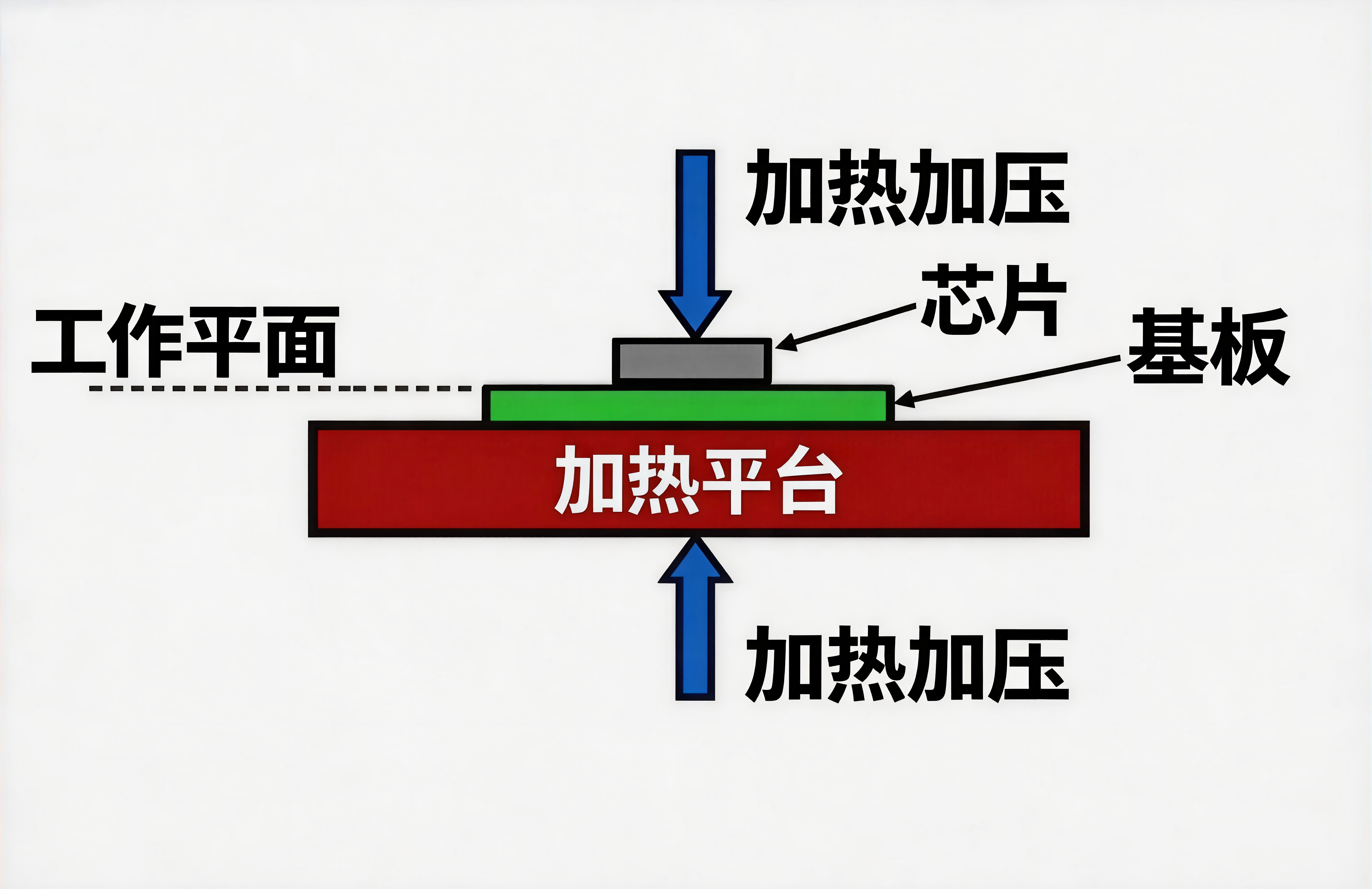
Key Parameters
- Workpiece Stage Temperature
- Nozzle / Fixture Temperature
- Heating / Cooling Rate
- Protective Atmosphere
Process Advantages
- Hermetic Packaging
- Lower Bonding Temperature vs. TCB
- One-Step Electrical & Mechanical Connection
- Meets Optoelectronic / RF High-Reliability Demands
Stamping
Stamping / Dip TransferA chip or dedicated stamping head is dipped into an adhesive pool to pick up a controlled amount, then transferred to the target position on the substrate. An efficient adhesive application method with highly uniform bondline thickness, especially suitable for multi-chip synchronous bonding, with precise control of adhesive coverage and fillet height. Key characteristic: area transfer, moderate adhesive volume, uniform coverage.
Key Parameters
- Dipping Depth
- Dwell Time
- Adhesive Pool Temperature
- Transfer Pressure
Process Advantages
- Highly Uniform Bondline Thickness
- High-Speed Multi-Chip Synchronous Application
- Precisely Controllable Adhesive Coverage
- Extremely Gentle on Thin / Fragile Chips
Pin Transfer
Pin TransferA precision pin array quantitatively picks up extremely small adhesive volumes from an adhesive pool, then precisely deposits them onto substrate target positions. A high-precision spot transfer process designed for ultra-small adhesive volume micro-assembly scenarios.
Key Parameters
- Pin Diameter
- Dipping Depth
- Transfer Speed
- Pin Temperature
Process Advantages
- Minimally Small & Precise Adhesive Volume
- Excellent Dot-to-Dot Consistency
- Compatible with Automated High-Speed Micro-Assembly Lines
Die Stacking
Die StackingChips are stacked layer by layer vertically with interlayer adhesive or bonding, maximizing area efficiency and minimizing signal path. A key technology for 3D / SiP packaging.
Key Parameters
- Stack Layer Count
- Interlayer Alignment Accuracy
- Interlayer Bondline Control
- Stacking Force Control
- Adhesive Squeeze-out & Fillet Control
- Ultra-Thin Chip Handling Strategy
Process Advantages
- Ultra-High Chip Density, Minimized Footprint
- Shortest Signal Path, Enhanced Frequency Performance
- Supports Multi-Layer Heterogeneous Integration
- Combinable with Flip Chip Technology
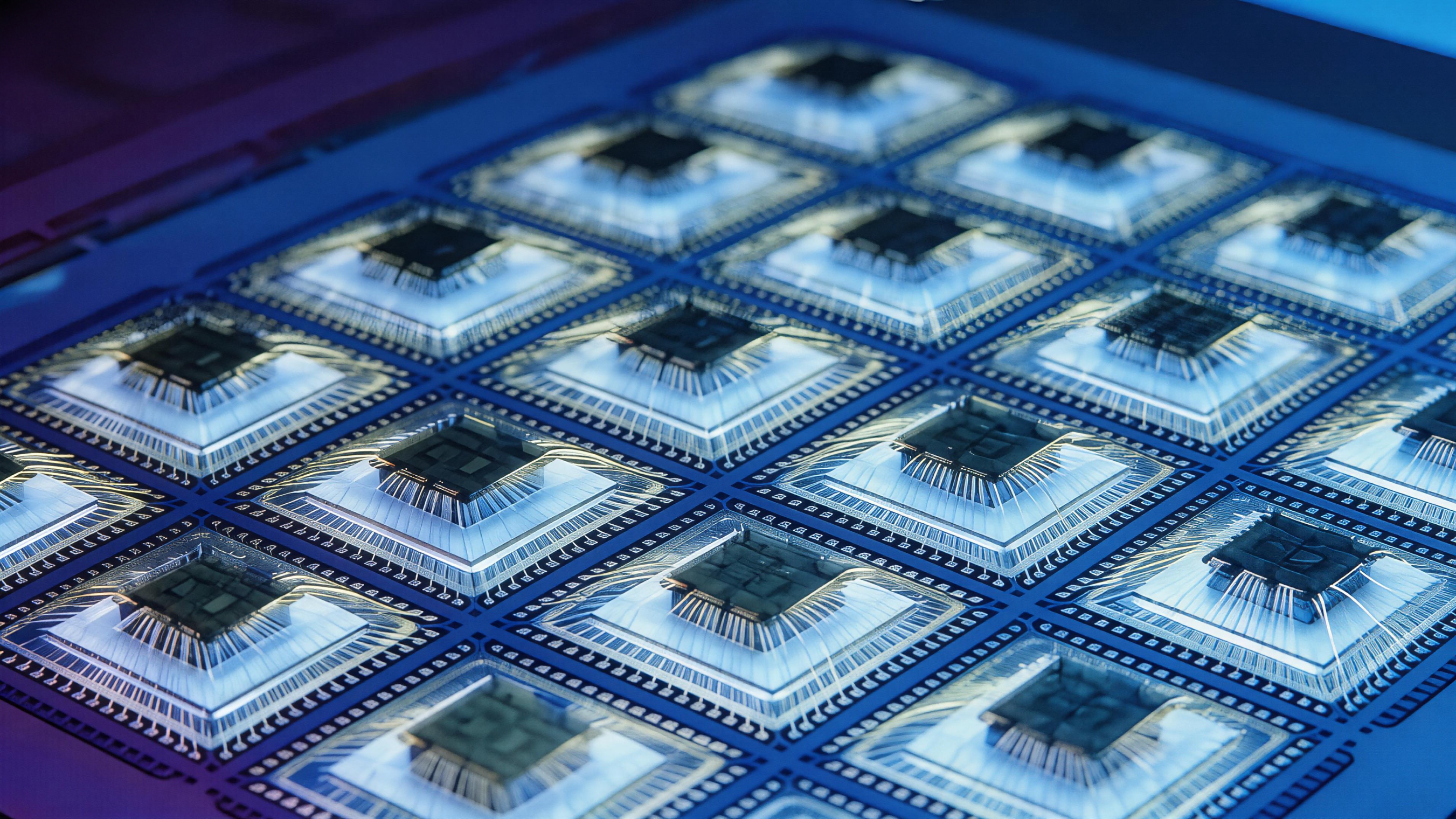
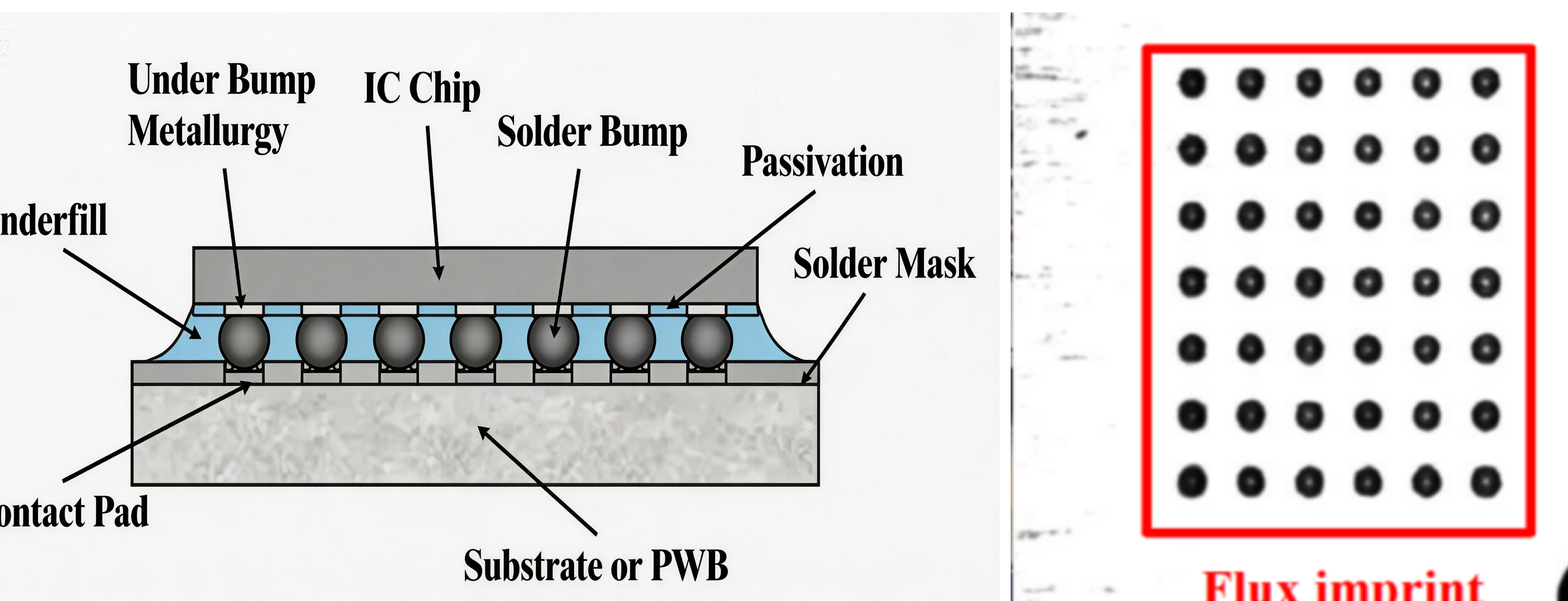
Flip Chip Bonding
Flip Chip BondingFlip chip bonding is a face-down, area-array interconnection technology where the chip's active surface is connected to substrate pads via bumps, achieving simultaneous electrical and mechanical interconnection. Compared to wire bonding's point-by-point connections, all interconnections are completed simultaneously with shorter signal paths and more compact packaging. Mainstream approaches include reflow, thermocompression bonding, and ultrasonic bonding.
Key Parameters
- Placement Accuracy
- Bump Type (C4 / Copper Pillar / Gold Stud)
- Bonding Method (Reflow / TCB / Ultrasonic)
- Flux Application Volume
Process Advantages
- Smaller Package: chip area = package area, 30–70% reduction
- Higher I/O Density: full area-array, thousands of bumps simultaneously
- Superior Signal Performance: mm to μm interconnect path, drastically reduced parasitic
- Higher Throughput: all connections simultaneously, independent of pin count
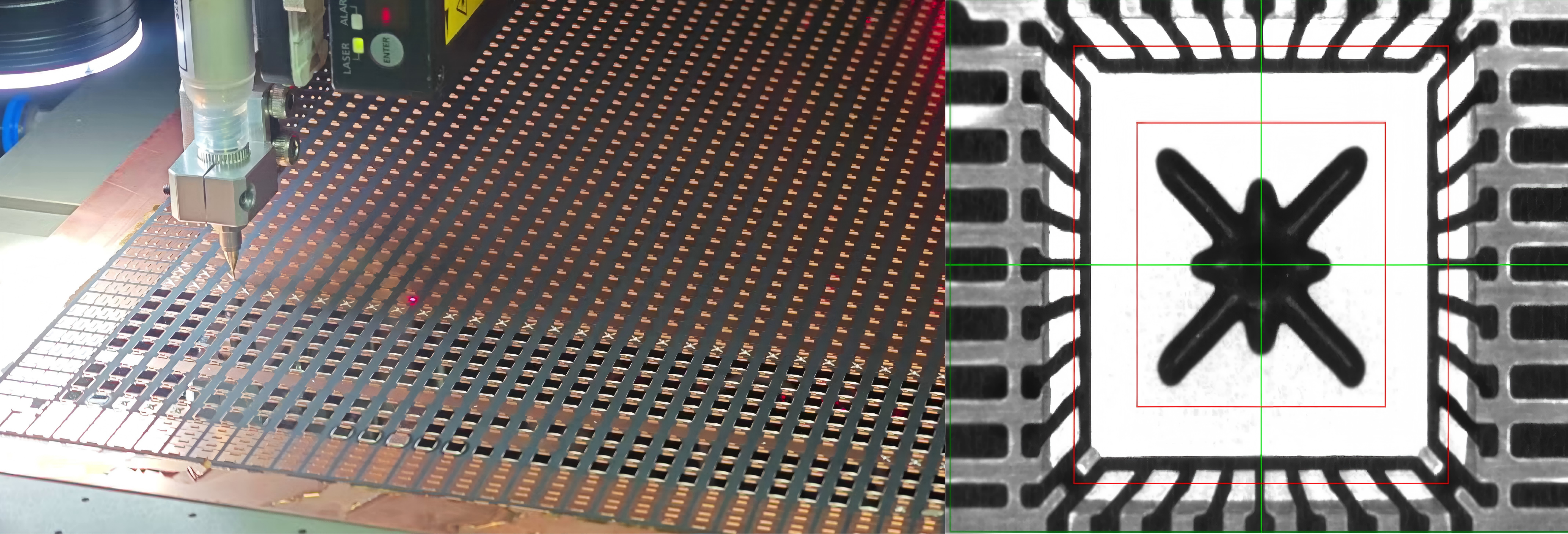
Die Sorting
Die SortingRe-arranges chips from wafer or other carrier sources into waffle packs, gel packs, or wafer film for organized feeding to subsequent die bonding operations.
Key Parameters
- Sorting Bin Mapping
- Pick Force Control
- Sorting Speed
- Vision Alignment Accuracy
Process Advantages
- Expanded Feeding Capacity for Multi-Chip Applications
- Structured Component Layout for Traceability
- Flexible Carrier Conversion
- Effectively Improves Bonding Throughput
UV Curing
UV CuringUV-curable adhesive cures within seconds upon ultraviolet irradiation. It remains liquid prior to UV exposure with unlimited pot life, allowing start/stop at any time with no material waste. Curing occurs at room temperature, with minimal thermal stress on substrates—suitable for inline production and temperature-sensitive devices. The adhesive locks components immediately after alignment, minimizing optical drift. Widely used in optical coupling alignment, lens bonding, and other precision assembly applications.
Key Parameters
- Adhesive Volume Control
- UV Wavelength (365 / 395 / 405 nm)
- UV Intensity & Exposure Time
Process Advantages
- Seconds-Level Curing, No Waiting
- Cures on Demand — No Adhesive Waste
- Low Thermal Stress — No Chip Damage or Alignment Drift
- Precise Adhesive Volume — No Optical Path Contamination
- Directly Embedded in Die Bonder Line — No Interruption
Ultrasonic Bonding
Ultrasonic BondingIt uses ultrasonic vibration and pressure to friction‑bond the chip to the substrate at room temperature – no heat required. Perfect for delicate components that don’t like heat or are hard to warm up.
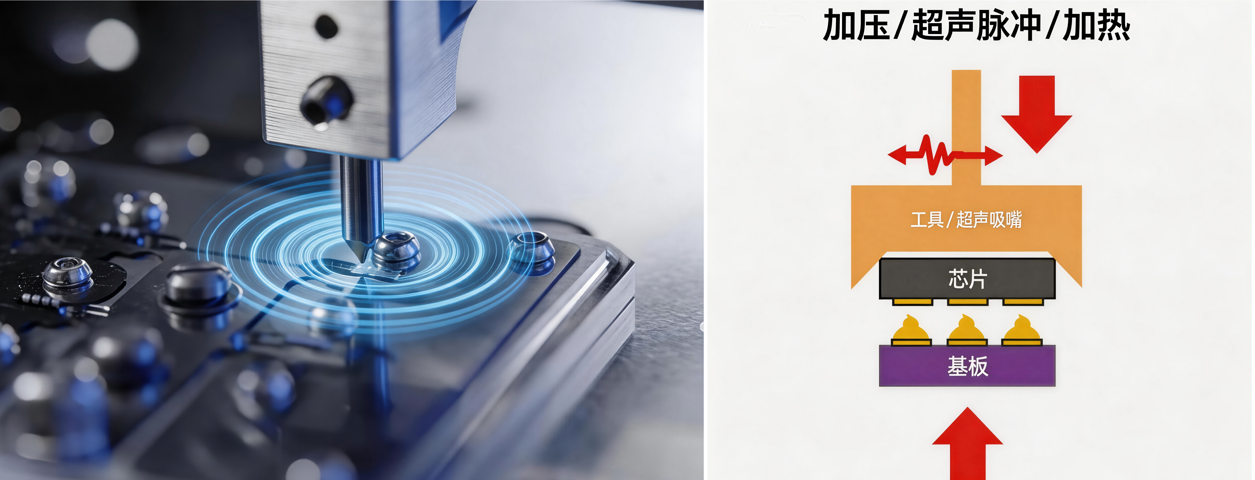
Key Parameters
- Bonding Force / Pressure
- Ultrasonic Power / Energy
- Frequency & Amplitude
- Ultrasonic Application Time
Process Advantages
- Room Temperature Bonding (optional heating, always lower than TCB)
- Short Bonding Time
- Excellent for Temperature-Sensitive Devices
- One-Step Conductive & Mechanical Connection