IBI Flip Chip Submicron Advanced Packaging
QX5000 Multi-Purpose Submicron Die Bonder | Indium Bump Flip Chip Bonding Application
Advanced Packaging

Indium Bump Interconnect Flip Chip Bonding

5–7 μm
Bump Diameter
15 μm
Bump Pitch
< 1 N
Bonding Force
Indium Bump Interconnect Flip Chip Bonding

I. Product & Process Applications

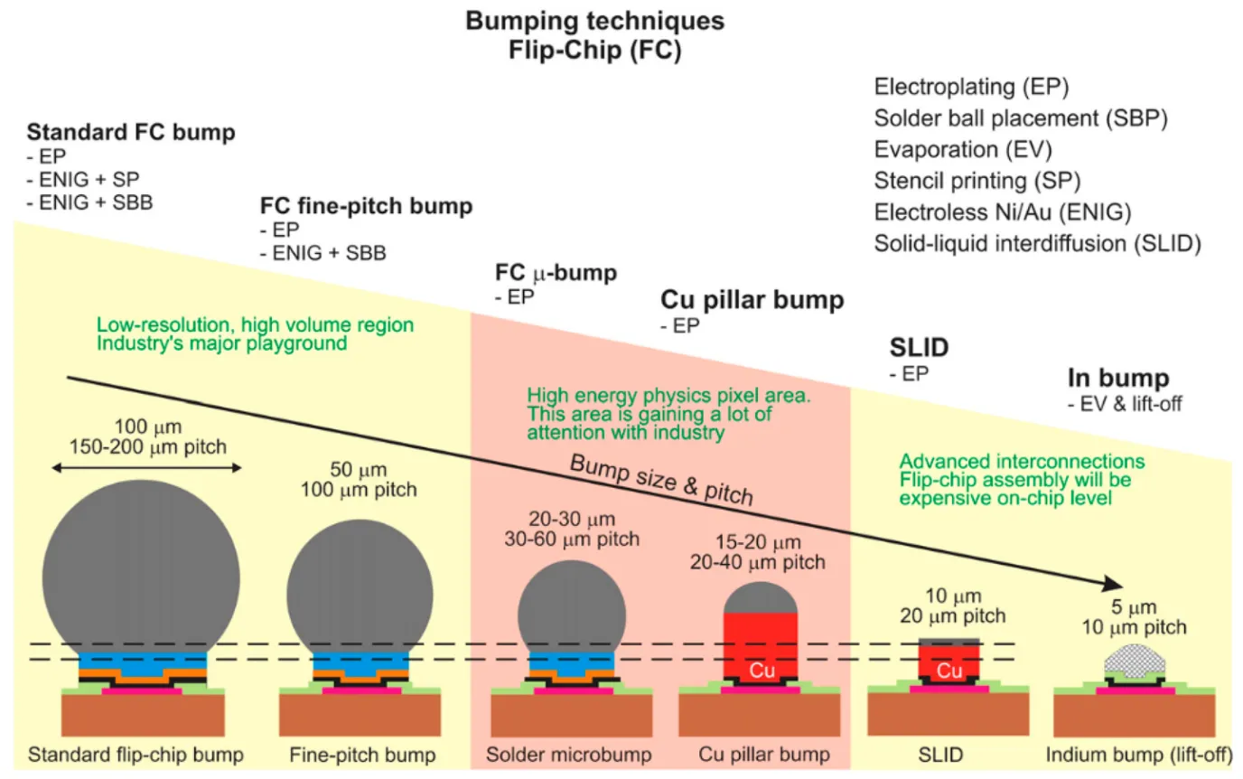
Indium Bump Interconnect (IBI) flip chip bonding is a critical process for achieving high-density interconnects in heterogeneous integration[1]. Primary applications include:

  • Infrared Focal Plane Arrays (IR FPA), X-ray Detectors, etc.: Hybrid integration of detector chips with readout integrated circuits (ROIC)
  • Quantum Computing Processors: 3D interconnect for superconducting qubits, such as compute and readout chip interconnects[3]
  • Micro LED Displays: High pixel density micro-display arrays, connecting LED chips with silicon CMOS drivers
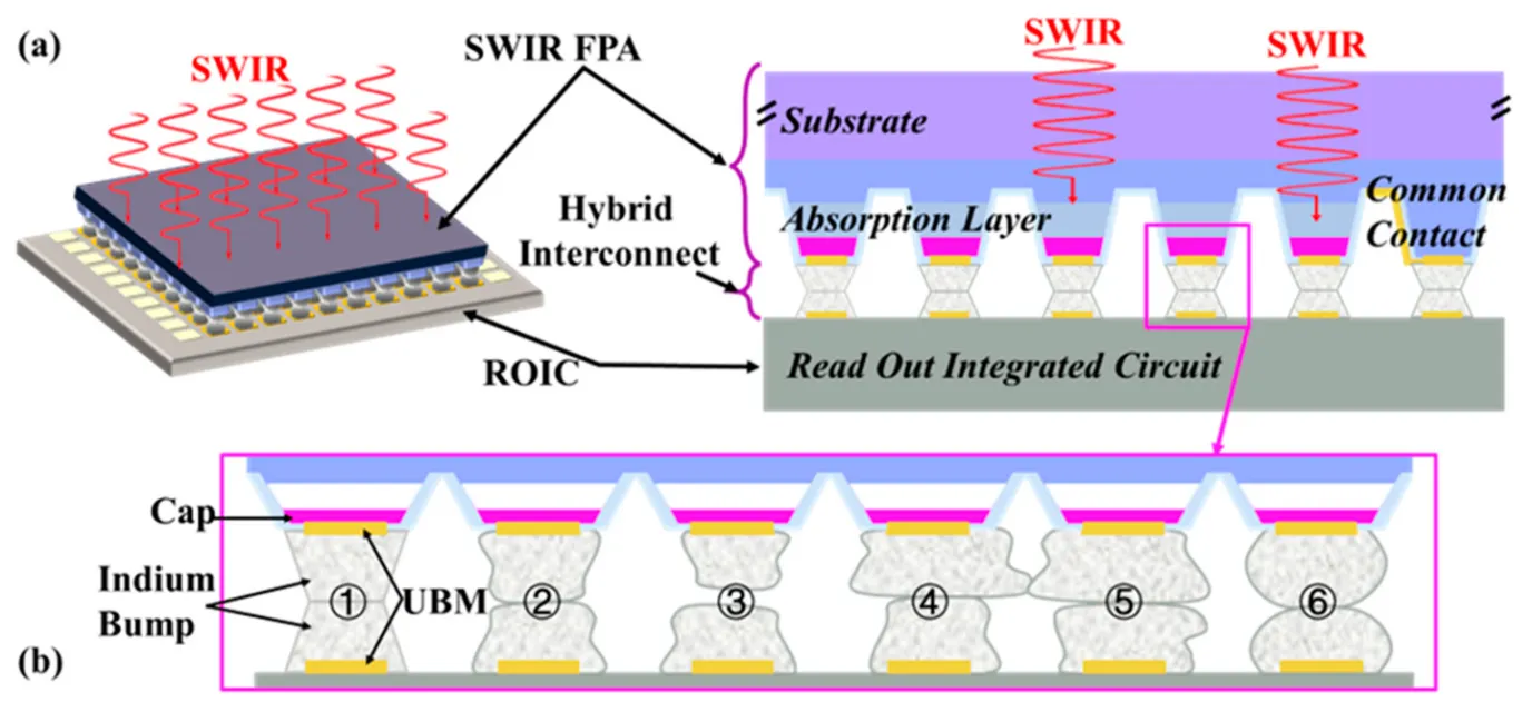
I. Product & Process Applications ▲ Indium bump interconnect flip-chip bonding structure diagram (SWIR FPA: Short-Wave Infrared Focal Plane Array)

II. Coplanarity Control

Indium bump array bonding requires all bumps to make simultaneous, uniform contact within the same plane[2]. Coplanarity errors of even a few microns across large-area chips (8×10 mm² or larger) cause uneven compression — some regions under-compress, causing opens, while others over-compress, causing shorts.

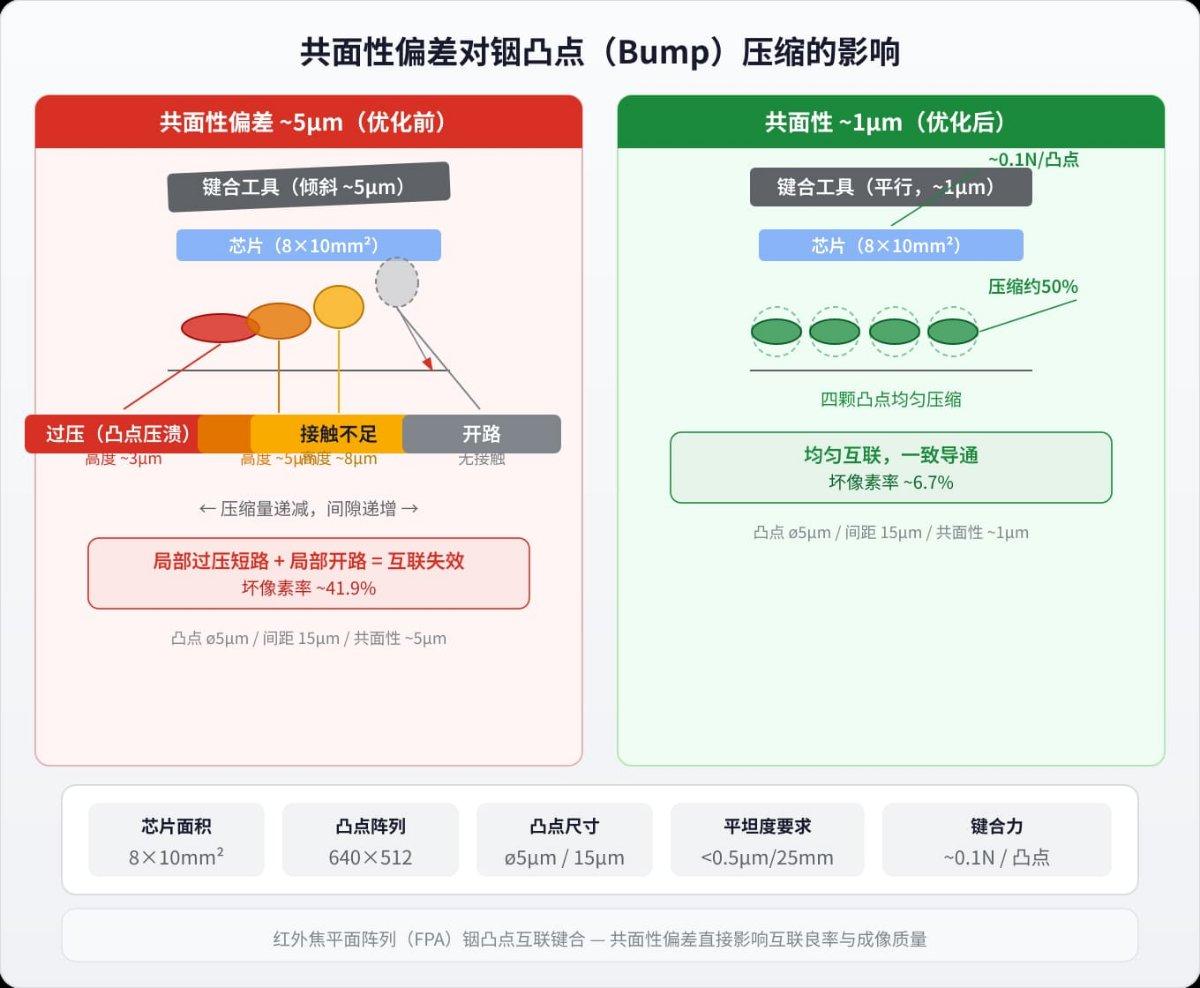
Coplanarity (Flatness) refers to the parallelism between the tool working surface and substrate surface during bonding. Even a 1 μm tilt causes differential bump compression across the chip, directly affecting interconnect yield and imaging quality. In IR sensor FPA bonding, coplanarity deviation manifests as fixed-pattern noise or dead pixel clusters[7].

  • Large-Format Case — IR FPA Flip Chip Bonding: Die size reaches 20–50 mm, nearly fully covering the indium bump array. For a 640×512 array with 5 μm bumps at 15 μm pitch across an 8×10 mm² area, overall flatness must be better than 1 μm — corresponding to tool leveling capability better than 0.5 μm per 25 mm. Coplanarity comparison observed through transparent chip: initial 5–6 μm error, optimized to ~1 μm.
  • Critical Role of Tool Material Selection: IBI flip chip bonding involves cold compression, thermocompression, and reflow processes — the bonding surface must meet < 0.5 μm/25 mm flatness. Tool materials must match the process: composite tungsten for cold compression to maintain flatness; copper-tungsten (CuW) for reflow/formic acid processes, leveraging its stable CTE and efficient thermal conduction to prevent bonding surface deformation during temperature changes.
II. Coplanarity Control ▲ Coplanarity deviation comparison observed through transparent chip: initial 5–6 μm (left) → optimized ~1 μm (right)

III. Bonding Process Requirements

Beyond coplanarity, IBI bonding faces equally critical challenges in ultra-low force control, material and surface management, and long-term precision stability. The choice among three bonding process types depends on the device's thermal sensitivity, material CTE matching, and available process window:

Table: IBI Bonding Process Types Comparison

Process TypeTypical Temp. RangeCore Physical/Chemical MechanismKey Purpose
Cold CompressionRoom temp ~ 90°CBelow indium melting point. Large mechanical force plastically deforms indium bumps, penetrating the surface oxide layer to form intimate mechanical and electrical contactAvoid thermal stress: critical for heat-sensitive devices or materials with severe CTE mismatch
Thermocompression100°C ~ 164°CNear but below indium melting point. Heat enhances atomic activity, enabling atomic bonding through thermally-activated diffusion under moderate pressureReduce bonding force: achieves reliable interconnect at lower force than cold compression
ReflowAbove 165°CComplete indium melting. Temperature exceeds indium melting point (156.6°C); bumps reflow into spherical shapes, forming robust metallurgical bondsBest electrical connection: re-solidified bumps exhibit the lowest contact resistance and best uniformity
Formic Acid Reflow210°C (reduction) / 165°C+ (reflow)Chemical reduction + physical melting. Two-step: ① 210°C — formic acid vapor reduces In₂O₃ to pure indium; ② 165°C+ — clean indium reflows above melting pointAddresses indium oxidation — the core challenge: in-situ oxide removal during bonding, without flux or plasma cleaning, significantly improving yield and reliability

Ultra-Low Force Control: 5 μm indium bumps are extremely fragile. Bumps must compress enough to form reliable interconnects without crushing into shorts. Cold compression bonding typically applies ~20 N/mm² across total bump area, compressing bump height by roughly 50%. Force per individual 5 μm bump is extremely low — pick-and-place and soft-contact stages require force control precision at the 0.05 N level. Practical pick-and-place forces range from 0.05 N to 1.0 N: too high crushes bumps; too low causes poor contact. Conventional limitation: standard die bonders typically start at 0.5 N, with step resolution insufficient for stable sub-0.1 N control, risking bump damage or open contacts.

Material & Surface Control: Indium oxidizes rapidly in air; the oxide layer blocks electrical continuity between bumps. Devices with temperature-sensitive structures or CTE-mismatched materials cannot use high-temperature reflow or formic acid de-oxidation, relying solely on cold compression bonding[4]. Meanwhile, the CTE mismatch between indium solder (In, melting point 156.6°C) and substrate/ROIC materials generates thermal stress during high-temperature processing, impacting low-temperature reliability. Particulate control is equally stringent — particles larger than 1 μm on the bonding surface can cause opens, directly affecting interconnect yield. Beyond pure indium, Au/In isothermal solidification is another low-temperature bonding route, suitable for thermally sensitive ceramic package scenarios[5][6].

Precision & Stability: IR sensor production requires multi-day continuous operation; equipment accuracy drift directly affects product imaging quality.
Process Challenge Overview

The following summarizes the seven core challenges in indium bump flip chip bonding, along with their quantitative targets and conventional solution limitations:

Table: Indium Bump Flip Chip Bonding Process Challenge Overview

ChallengeQuantitative DescriptionConventional Solution Limitations
Submicron Alignment Accuracy5 μm bumps, 15 μm pitch array alignment requires <0.5 μm (3σ), CPK ≥ 1.67Production bonders targeting >25 μm pitch typically offer ±3–10 μm accuracy, insufficient for fine-pitch arrays
Coplanarity ControlWithin bonding area (e.g., 8×10 mm²), coplanarity must be <1 μm, requiring tool leveling capability <0.5 μm/25 mmEquipment without precision leveling mechanisms struggles to ensure uniform contact over large areas
Bond Line Thickness ControlBump height 5–7 μm; post-bond solder layer only 2–4 μm, must be uniformImprecise force control leads to local over-compression or poor contact
Ultra-Low Force ControlFine-pitch indium bumps are extremely fragile; pick-and-place force must reach 0.05 N levelStandard die bonders typically start at 0.5 N force range
Material MatchingCTE mismatch between chip (e.g., GaAs, 5.73–6.86 ppm/K) and ROIC (Si, 2.6 ppm/K)High-temperature processes prone to thermal stress failure
Special EnvironmentIR sensors must operate stably under cryogenic conditionsConventional bonding processes struggle to guarantee low-temperature reliability
Surface Oxidation & ContaminationIndium surface oxidizes rapidly; particles >1 μm can cause opens; some devices prohibit flux, precluding flux or formic acid processesOxidation is difficult to control without gas protection environment

These seven challenges span the entire IBI bonding workflow, demanding systemic equipment-level capabilities — not isolated point solutions.

IV. Solution

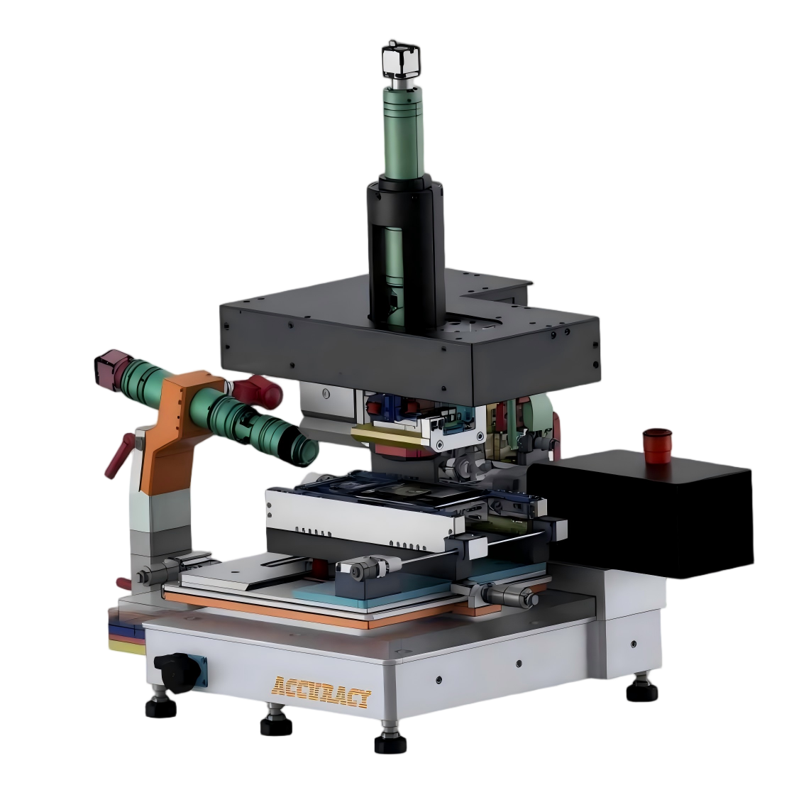
To address the above challenges, Accuracy's QX5000 provides systemic capabilities across multiple dimensions — accuracy, force control, thermal control, atmosphere, and process compatibility: ±0.5 μm
1. Placement accuracy with dual-camera vision system (FOV 0.5×0.6 mm ~ 6×7.2 mm) + air-bearing motion platform + full closed-loop control algorithm;
2. Workstage flatness meets submicron requirements with fine adjustment (θ-axis range ±5°); customizable passive self-leveling pickup tool achieves adaptive leveling, correcting coplanarity to < 0.5 μm over 25 mm tool surface;
3. Bonding force range 0.1 N–30 N, covering the ultra-low force range required for indium bump bonding;
4. Heating temperature: up to 450°C ± 1°C, ramp-up 20°C/s, cool-down 5°C/s, bonding surface temperature uniformity < ±1°C, covering the full temperature range from cold compression to formic acid reflow;
5. Process compatibility: supports cold compression, thermocompression, eutectic soldering, flip chip/face-up die attach on a single platform; configurable with N₂ carrier gas + formic acid vapor module for in-situ oxide reduction at the bonding zone.

QX5000's indium bump bonding capabilities have been verified through parameter benchmarking:

Table: QX5000 vs IBI Requirements — Parameter Benchmark

ParameterQX5000 CapabilityIBI Typical RequirementResult
Placement Accuracy±0.5 μm<0.5 μm @ 3σ, CPK ≥ 1.67✅ Meets
Coplanarity<0.5 μm/25 mm<0.5 μm/25 mm✅ Meets
Temperature RangeRT–450°C ± 1°CRT / 165°C / 210°C✅ Meets
Ramp-Up / Cool-Down20°C/s / 5°C/sRapid thermal cycling✅ Meets
Bonding Force0.1 N–30 N<1.0 N pickup force✅ Covers
Process GasN₂ / Formic Acid (optional)N₂ / Formic Acid environment✅ Available
Process TypeFC / Face-Up / Stack / CoG / CoFFlip chip bonding✅ Supported

All seven core parameters meet or exceed IBI requirements — with particularly strong matches on ±0.5 μm accuracy, < 0.5 μm/25 mm coplanarity, and 0.1 N ultra-low force control.

V. Process Development

The challenge of indium bump bonding lies in simultaneously meeting four dimensions: accuracy, force control, thermal control, and environmental control. QX5000 integrates ±0.5 μm accuracy, 0.1 N fine-force control, 450°C heating, and gas protection on a single platform — capable of addressing diverse indium bump flip chip bonding needs, from IR sensors to quantum processors.

From micron to submicron, from single to multi-dimensional — precision interconnect, driving limitless possibilities for next-generation optoelectronics.

If you are evaluating or developing indium bump bonding related products, we welcome process trials and on-site demonstrations.

±0.5 μm Accuracy 0.1 N–30 N Force 450°C ± 1°C
艾科瑞思

Suzhou Accuracy Intelligent Equipment Co., Ltd., founded in 2010 and headquartered in Suzhou Industrial Park, is a professional supplier of high-precision advanced semiconductor packaging equipment, dedicated to the research, design, manufacture, and sale of high-accuracy, high-throughput, high-reliability, and intelligent die bonding systems.

With 16 years of deep industry experience, Accuracy provides next-generation die bonding equipment for emerging semiconductor materials and advanced packaging processes — including multi-chip die bonders for system-in-package (SiP), die sorters, wafer-level hybrid bonders (Chip-to-Wafer Hybrid Bonder with 200 nm alignment accuracy, becoming the first Chinese D2W equipment supplier recognized in the Yole Group 2025 report; project fully divested), and flip chip bonders — serving customers across advanced packaging, IC assembly, RF/microwave, optoelectronics, and sensor markets with professional die bonding solutions.

艾科瑞思
References
  • [1]Travis Scott, Finetech GmbH & Co. KG. Indium Bump Interconnect (IBI) Flip Chip Bonding[R]. Technical Paper, 2024.
  • [2]Lucas T J, Biesecker J P, Doriese W B, et al. Indium Bump Bonding: Advanced Integration Techniques for Low-Temperature Detectors and Readout[J]. Journal of Low Temperature Physics, 2024, 216: 67–72.
  • [3]Norris G J, Michaud L, Pahl D, et al. Improved parameter targeting in 3D-integrated superconducting circuits through a polymer spacer process[J]. EPJ Quantum Technology, 2024, 11(5).
  • [4]Fritzsch T, et al. Investigation of low temperature bonding process using indium bumps[R]. Fraunhofer IZM / CERN Indico, 2018.
  • [5]Shen W J. Low-temperature bonding method based on Au/In isothermal solidification[P]. Chinese Patent: CN106298557B, 2019-08-02.
  • [6]Shi J Z, Wang T B, Xie X M. Application of Au/In alloy in ceramic package die attach[J]. Journal of Functional Materials and Devices, 2000, 6(2): 119–124.
  • [7]Du J, Zhao X, Su J, et al. Review of Short-Wavelength Infrared Flip-Chip Bump Bonding Process Technology[J]. Sensors (Basel, Switzerland), 2025, 25(1): 263.