Process Challenges
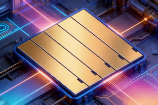
Laser bars — arrays of edge-emitting semiconductor emitters — are the fundamental building blocks of high-power diode lasers, widely deployed in solid-state laser pumping, medical systems, and materials processing. As industrial laser power levels continue to climb, laser bar packaging faces mounting challenges in thermal management, placement accuracy, and stress control.
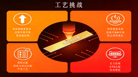
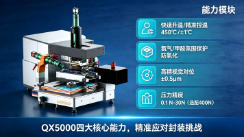
- Thermal Management: As operating temperatures and optical power densities continue to rise, chip heat dissipation demands grow. The heating module must rapidly reach above 300°C and cool quickly to minimize cycle time. The bonding environment requires effective oxidation prevention — otherwise solder joint quality is compromised. For large heatsinks with significant thermal losses, dedicated tooling must be designed to reduce heat conduction into the equipment.
- Placement Accuracy: The laser bar emission edge must be precisely aligned with the heatsink edge, with overhang controlled within 5–10 μm — a parameter that directly determines yield. This places extreme demands on the die bonder's alignment precision.
- Solder-Chip Compatibility: Laser bar packaging predominantly employs Au80Sn20 (gold-tin) eutectic solder (melting point 280°C), which delivers the best thermo-mechanical reliability and corrosion resistance — the preferred choice for high-reliability assemblies. However, its process window is extremely narrow: highly sensitive to temperature profiles and atmospheric conditions, and the large CTE mismatch between the solder and the GaAs chip makes bonding stress control exceptionally difficult. To balance stress against reliability, some designs opt for indium (In) solder (melting point 157°C), leveraging its softness to buffer thermal mismatch stress; others adopt nano-silver sintered paste for superior thermal conductivity and thermal-fatigue life. Solder selection ultimately represents a comprehensive trade-off among cost, performance, and process complexity.
- Stress Control: The laser bar is made of brittle GaAs, whose CTE mismatches that of the heatsink (typically CuW or AlN). Bonding-induced stress can cause bar bowing, dark-line defects, or even chip fracture, requiring effective mitigation measures.