Process Challenges
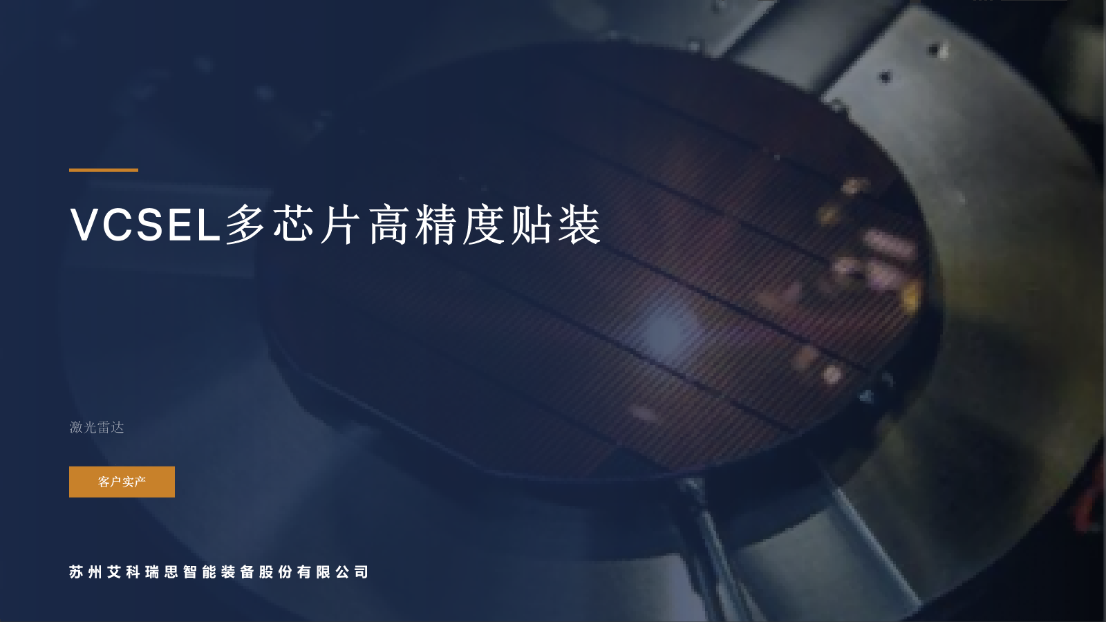
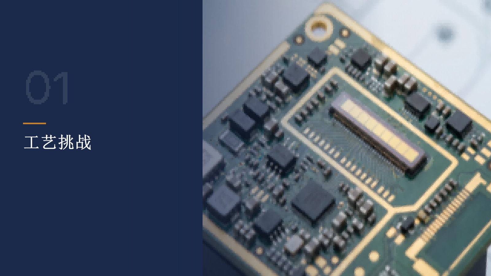
The customer specializes in VCSEL chip (GaAs substrate) R&D and manufacturing, producing emitter devices for automotive LiDAR. Chip size is below 0.15 mm, thickness below 100 μm, supplied on blue film. Multiple VCSEL array chips are bonded as a whole onto a PCB substrate.
- Small-chip Pickup: Ejector pin operations easily cause blue film tearing and chip damage/fracture
- Small-chip Recognition: Vision recognition stability for tiny array chips is poor, prone to recognition failures
- Strict Dispensing Requirements: Sidewall fillet must cover over 70%, with full perimeter wet-out; actual production is prone to adhesive pullback