Low-Temperature, Flux-Free VCSEL Flip-Chip: A Thermosonic Route Case
Ultrasonic bonding is a bonding technique that uses pressure and high-frequency mechanical vibration energy to plastically deform the metal interface and form a solid-state joint. Its advantages are solder-free, lower required temperature and pressure, and faster bonding rate; it is commonly used for gold-bump (Au bump) flip-chip.
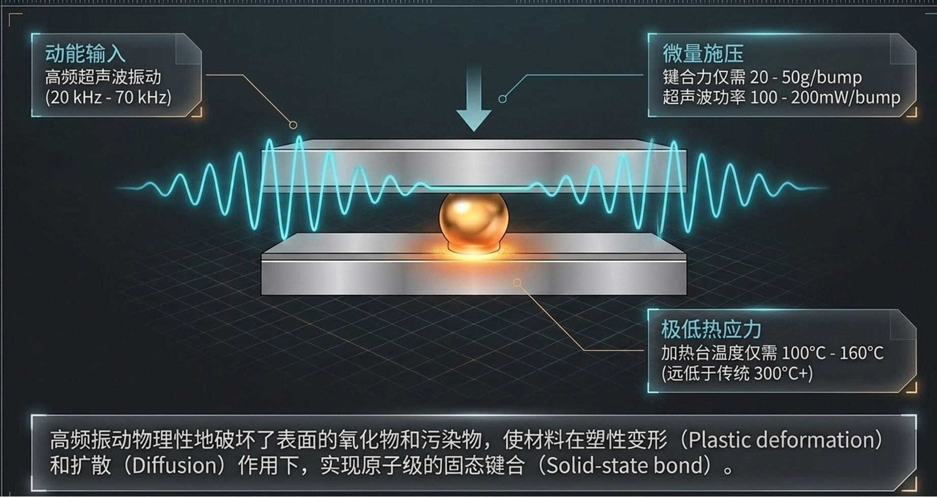
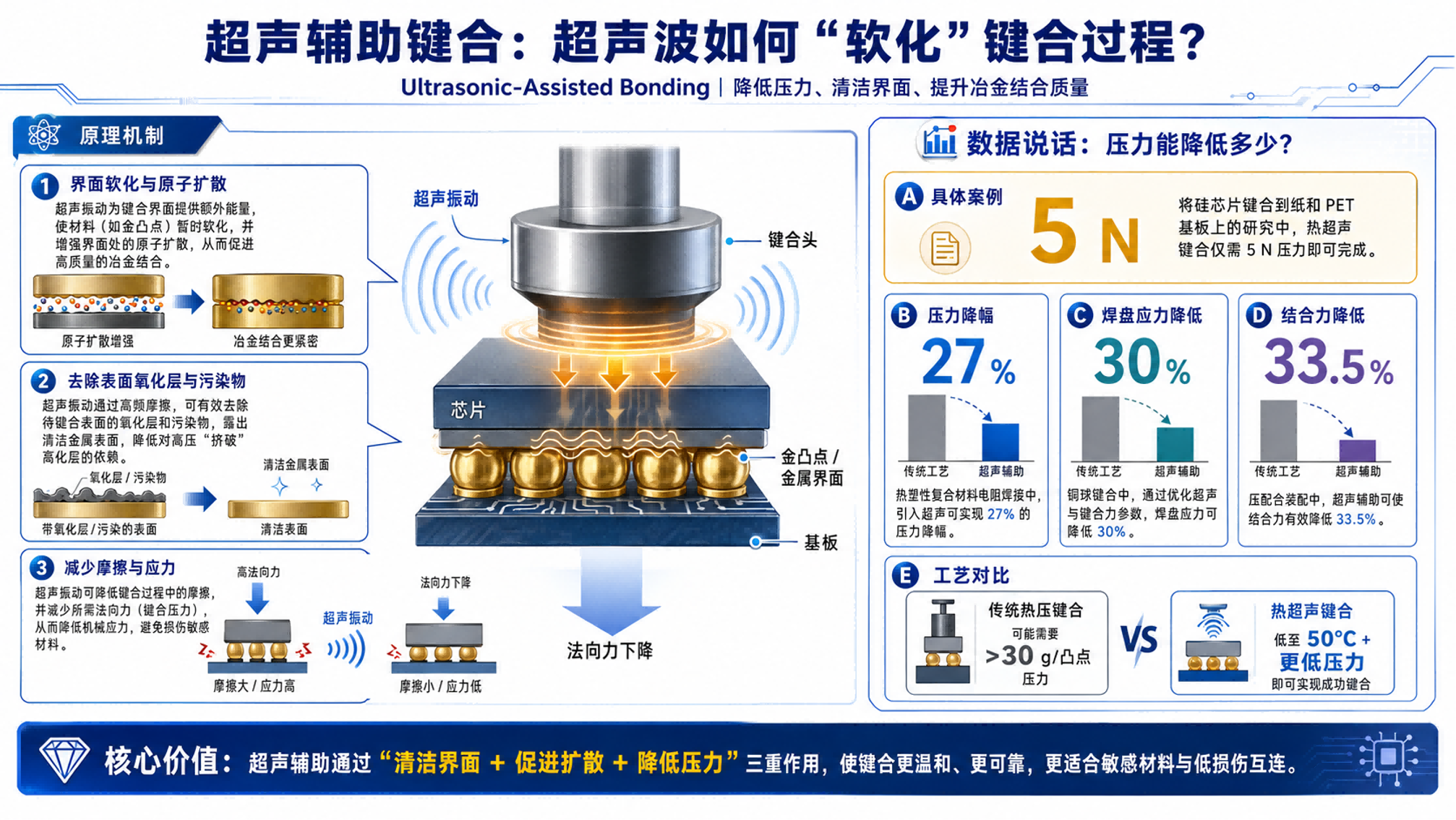
Adding moderate heating on top of ultrasonic bonding gives thermosonic bonding (Thermosonic Bonding) — similar to thermocompression, but the introduced ultrasonic energy markedly lowers bond force and temperature. Pure thermocompression often needs >300°C; thermosonic, combining thermocompression + ultrasonic welding, brings temperature and force down to below 200°C, 20–50 g/bump, targeting placement scenarios sensitive to temperature and demanding on interface cleanliness, achieving a gentle, reliable, high-precision microelectronic connection.
一、Application Case: VCSEL and Glass Interposer Precision Interconnect
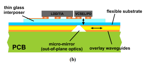
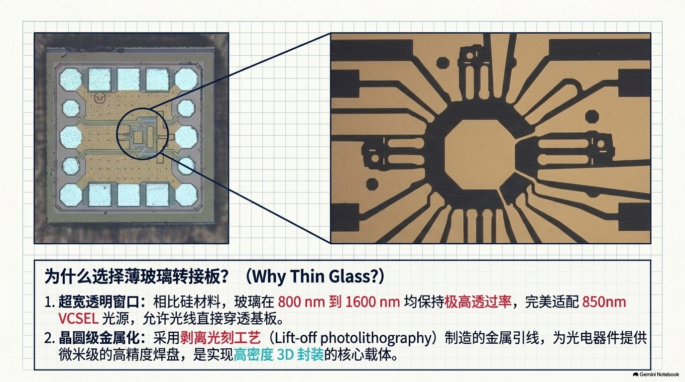
In board-level optical interconnect, VCSEL and PD convert between electrical and optical signals. To shorten the electrical-interconnect path and couple the beam into the on-board polymer waveguide, the optoelectronic chip can be flip-chipped onto a transparent glass interposer first, then integrated with driver/receiver circuits and the waveguide structure. This step must complete electrical connection while also handling optical-surface cleanliness, device placement, and post-bond stability.
This study used Au stud bump thermosonic flip-chip to interconnect the VCSEL with the glass substrate. The test assembly used 3 gold bumps, completed at 120°C, total force 1 N, ultrasonic power 1 W, pulse 500 ms. The flux-free solid-state process helps reduce residue risk near the optical coupling surface, and the lower temperature with shorter action time also leaves room to control assembly thermal input.
二、Ultrasonic Bonding Challenges: Align, Withstand, Flatten
Challenge ① · Place it accurately, and keep it from shifting after bonding
The light emitted by the VCSEL must align to the micro-mirror and then enter the waveguide. Even if placement is accurate, bump compression and ultrasonic micro-vibration during bonding may shift the die slightly; once the offset is too large, less light enters the waveguide. Therefore, high placement accuracy is required, and more importantly, the actual post-bond accuracy and optical-coupling effect must be examined.
Challenge ② · Precise control of temperature, pressure, and ultrasonic parameters
If temperature, pressure, or ultrasonic energy is insufficient, the gold bump may not bond firmly; if parameters are too high, the bump may over-deform and even raise the risk of chip and thin-glass damage. Process development must tune temperature, pressure, ultrasonic power, and duration together to find a window that bonds firmly without over-stressing.
Challenge ③ · Flatness control of multiple bumps: simultaneous contact, uniform force
Multiple gold bumps are like the legs of a table: if one is too high or too low, or the collet is not flattened, one side may already be pressed while the other has not yet contacted. Before assembly, bump-height control is needed and the collet must stay parallel to the substrate so every joint connects stably.
Solution
For low-I/O requirements, Accuracy QX5000 can provide an ultrasonic bonding solution:
- ±0.5μm standard-die placement accuracy — an in-house vision system supports ±0.5μm standard-die placement accuracy, with what-you-see-is-what-you-get visual support during placement
- Temperature–force coordinated control — 0.1–30 N bond force with up to 450°C stage heating, letting you validate around contact force, temperature, and duration to find the window between joint strength and device protection
- Configurable ultrasonic module — for Au stud bumps and compatible pad metallization, an ultrasonic transducer, dedicated tools, and process parameters can be configured per project
- Custom collet fixtures — Die Collet and fixtures customized to chip size, emission area, bump count, and glass-substrate structure, integrating a coining (flattening) function for pick-place protection, clamping rigidity, and uniform force
- Traceable, reproducible placement — the equipment records per-die process parameters and supports in-process observation
Move Sensitive Optoelectronics' Low-Temperature Clean Interconnect from Drawing to Prototyping
Submit your product information and our process team will evaluate a suitable interconnect solution and arrange sample validation.
Book Process Test →Accuracy (Suzhou Accuracy Intelligent Equipment Co., Ltd.), founded in 2010 and headquartered in Suzhou Industrial Park, is a specialized supplier of high-precision advanced semiconductor packaging equipment, focused on the R&D, design, manufacturing and sales of high-precision, high-speed, high-reliability and intelligent die-bonding systems.
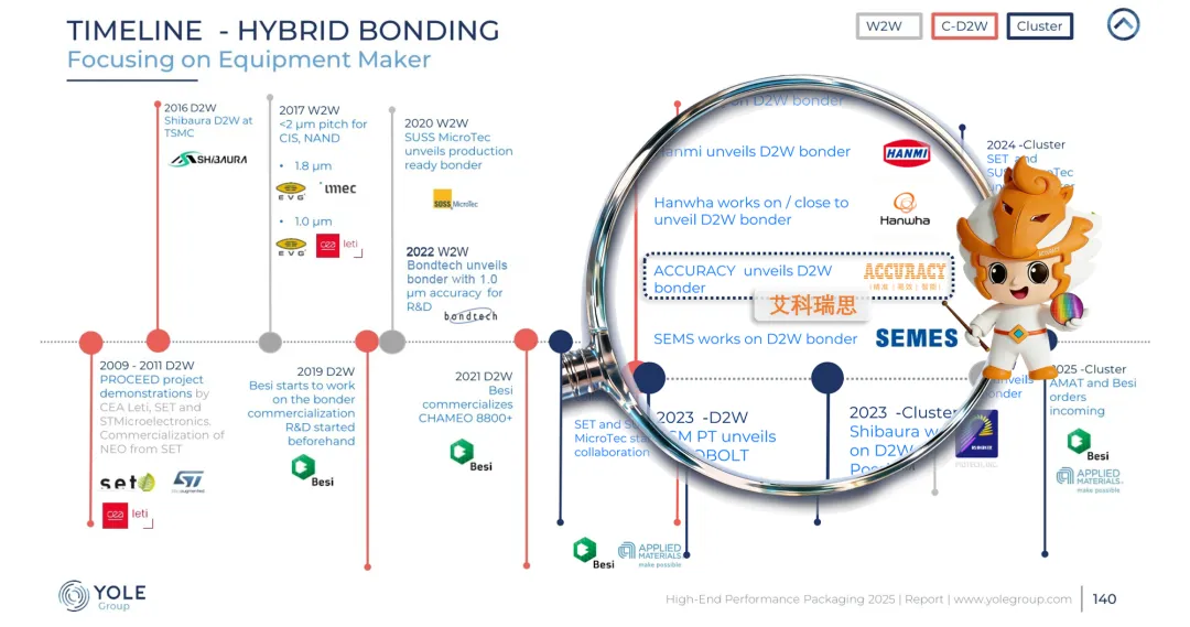
After 16 years of industry dedication, Accuracy provides a new generation of die-bonding equipment for emerging semiconductor materials and advanced packaging processes — including System-in-Package (SiP) multi-chip die bonders, sorters, wafer-level hybrid bonders (Chip-to-Wafer Hybrid Bonder, alignment accuracy 200 nm, becoming China's first D2W equipment supplier listed in the Yole Group 2025 report) and flip-chip die bonders — serving professional die-bonding solutions for advanced packaging, IC assembly, RF/microwave, optoelectronics and sensor markets.
Some images and data on this page are cited from public academic literature and public reports, for popular-science purposes only.
References
- [1] Nieweglowski K, Tiedje T, Schöniger D, et al. Electro-optical Integration for VCSEL-Based Board-Level Optical Chip-to-Chip Communication. Proceedings of SPIE, 10325, 103250V (2017). DOI: 10.1117/12.2271046.
