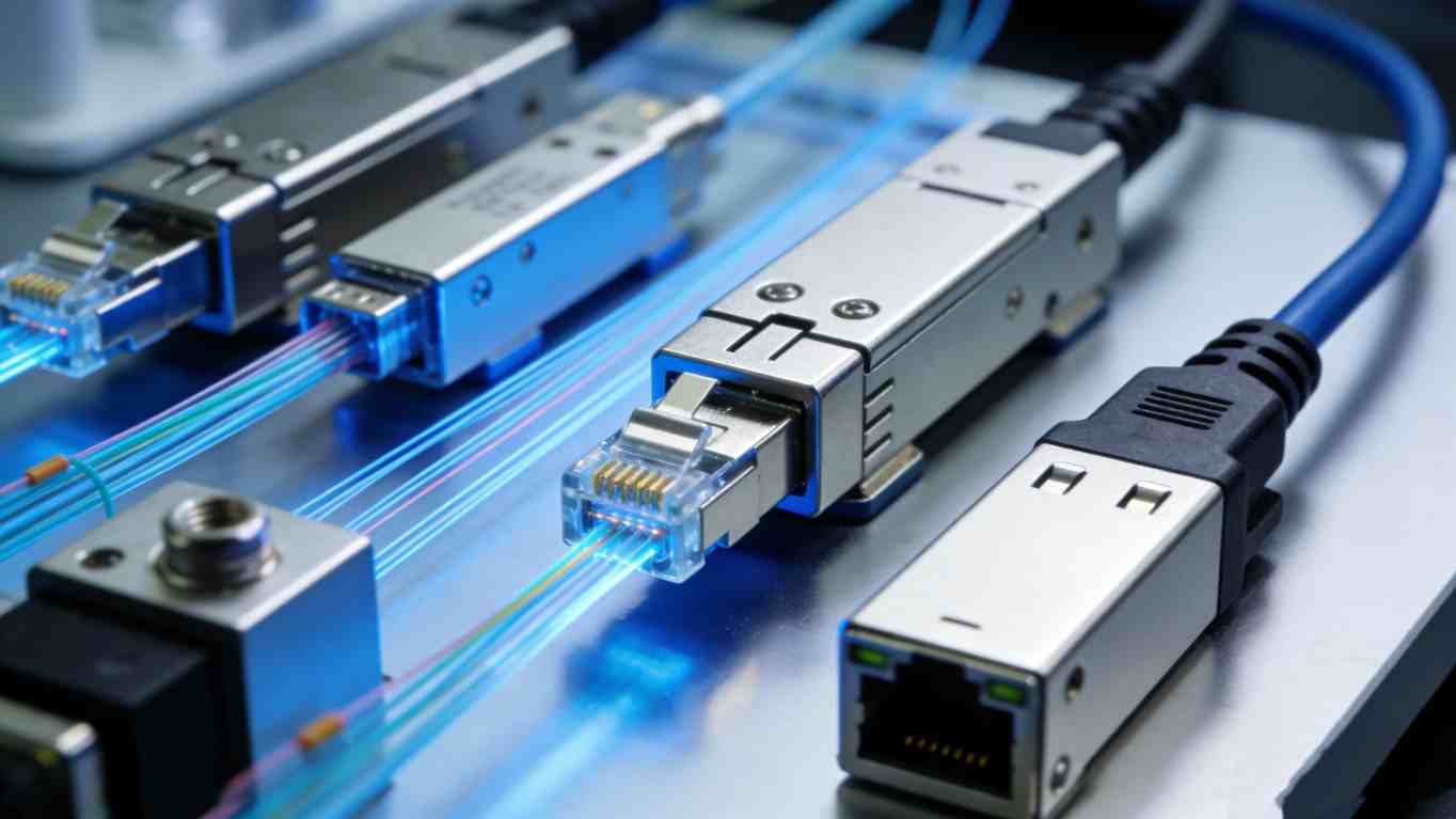
SiP Packaging
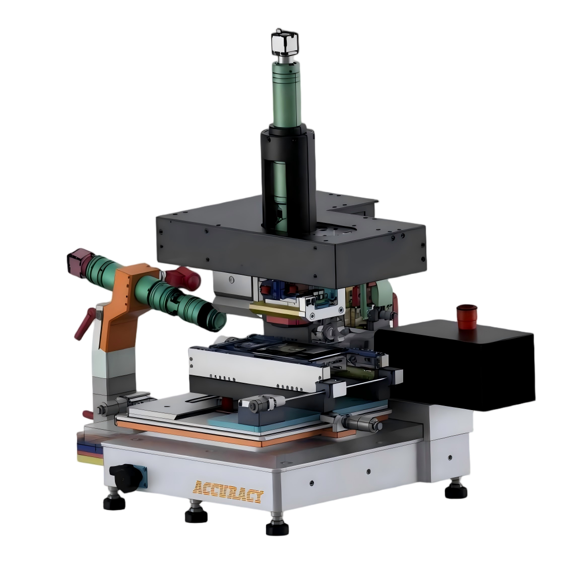
SiP Multi-Chip Die Bonder Expert
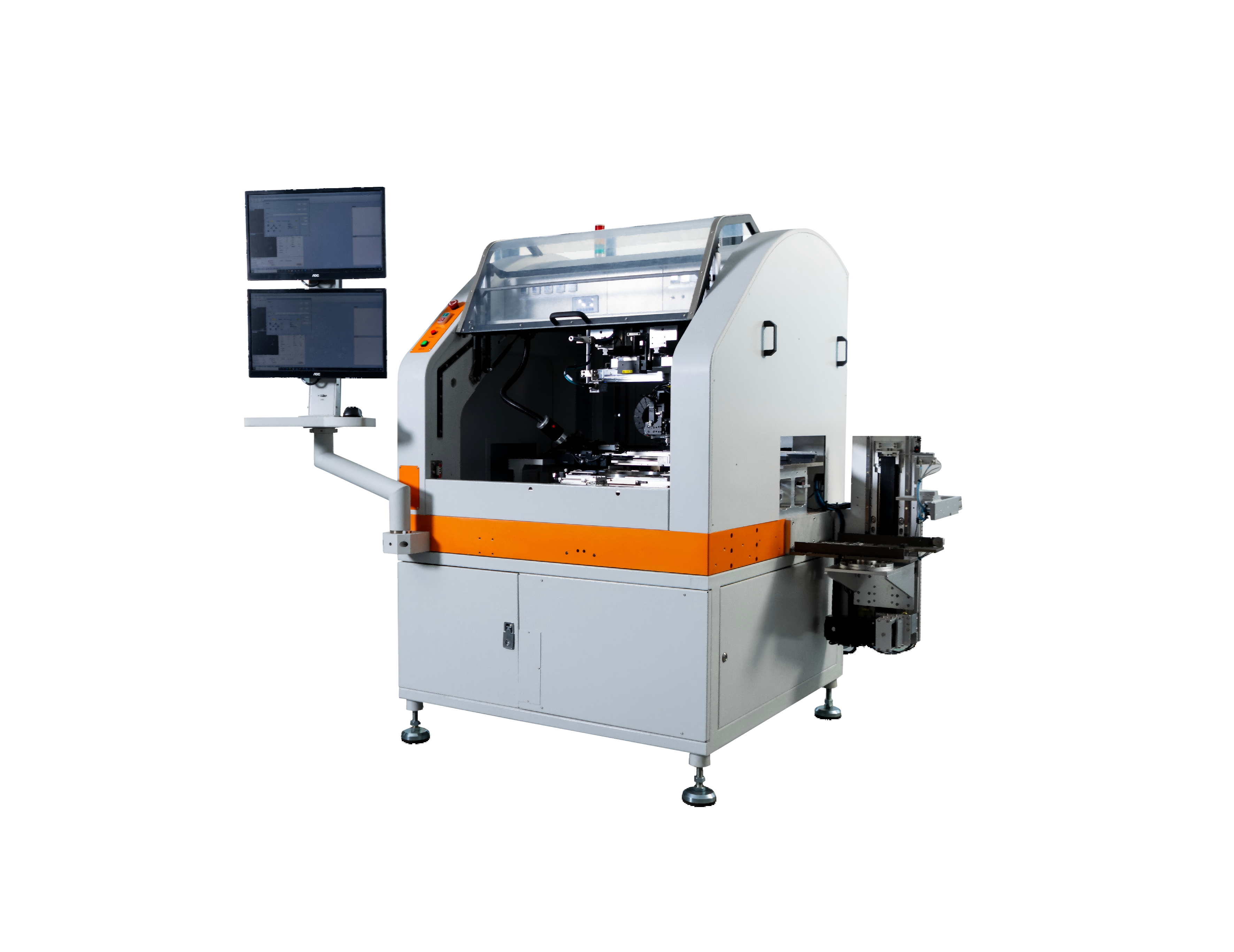
ZX2200
SiP Multi-Chip High-Precision Die Bonder
ZX2200 / ZX2200 plus / ZX2200 evo adv
±3μm Accuracy · Multi-Process Platform · Purpose-Built for SiP Multi-Chip Bonding
±3/7/10μm
Placement Accuracy
≥1,200
Throughput (UPH)
Max 12"
Wafer Size
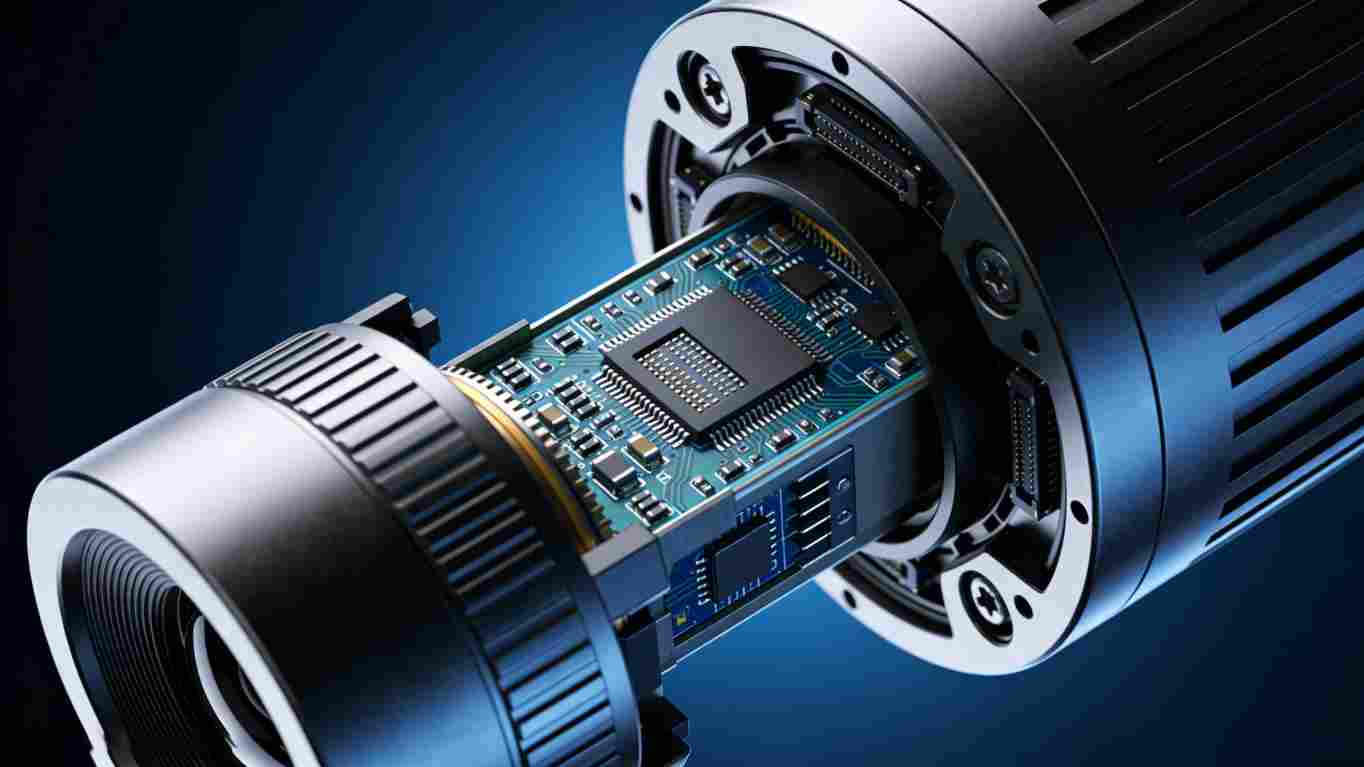
ZX2200 evo adv — ACCURACY's latest SiP multi-chip high-precision die bonder with ±3μm accuracy. Designed for optical, microwave/RF, LiDAR, and MEMS packaging.
Modular architecture supports wafer, waffle, and gel pack feeds, and processes dispensing, stamping, and flip-chip bonding — enabling multi-process flexibility and fast changeover in one machine.
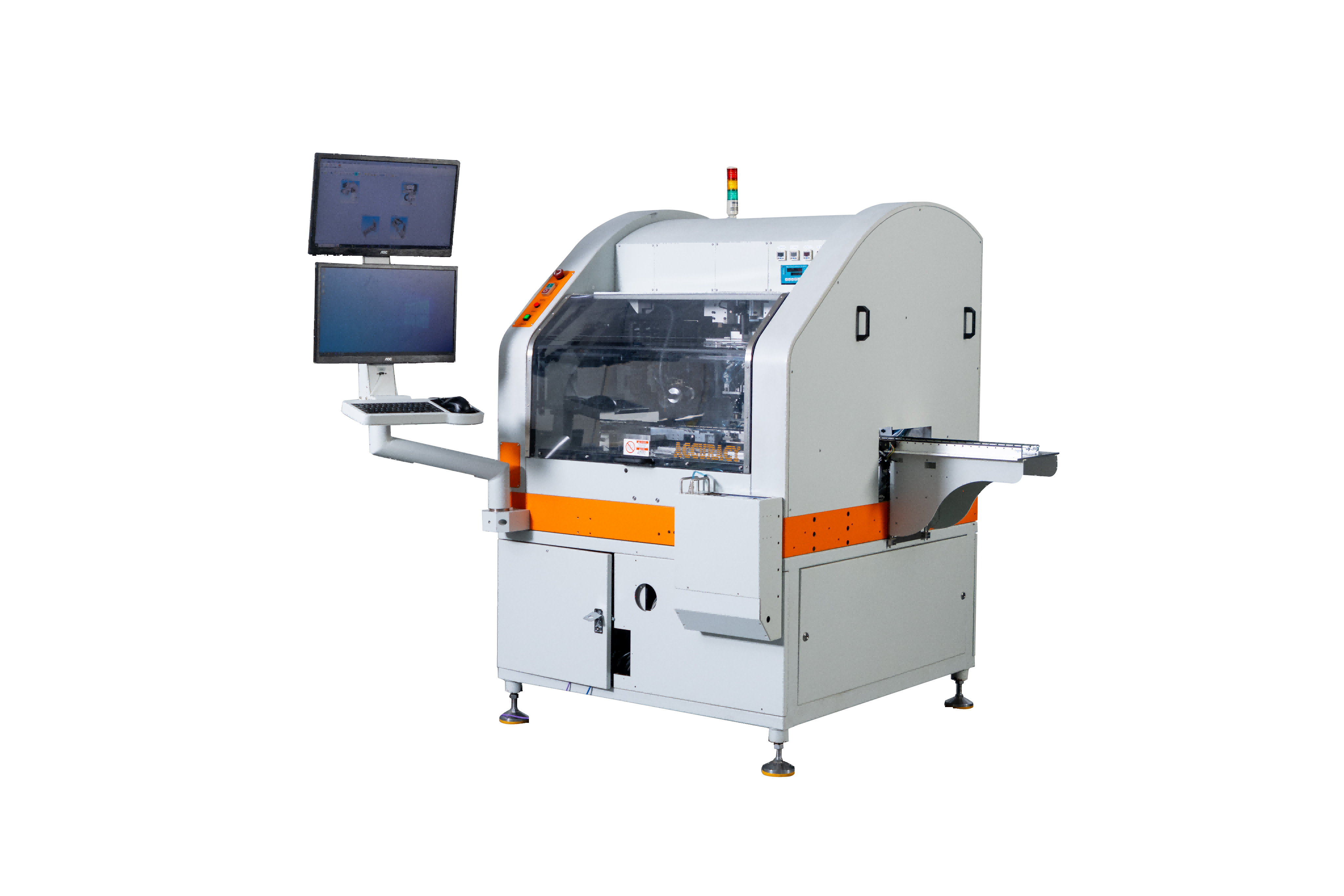
ZX2200 SiP Module Multi-Chip High-Precision Die Bonder 细节图
Front
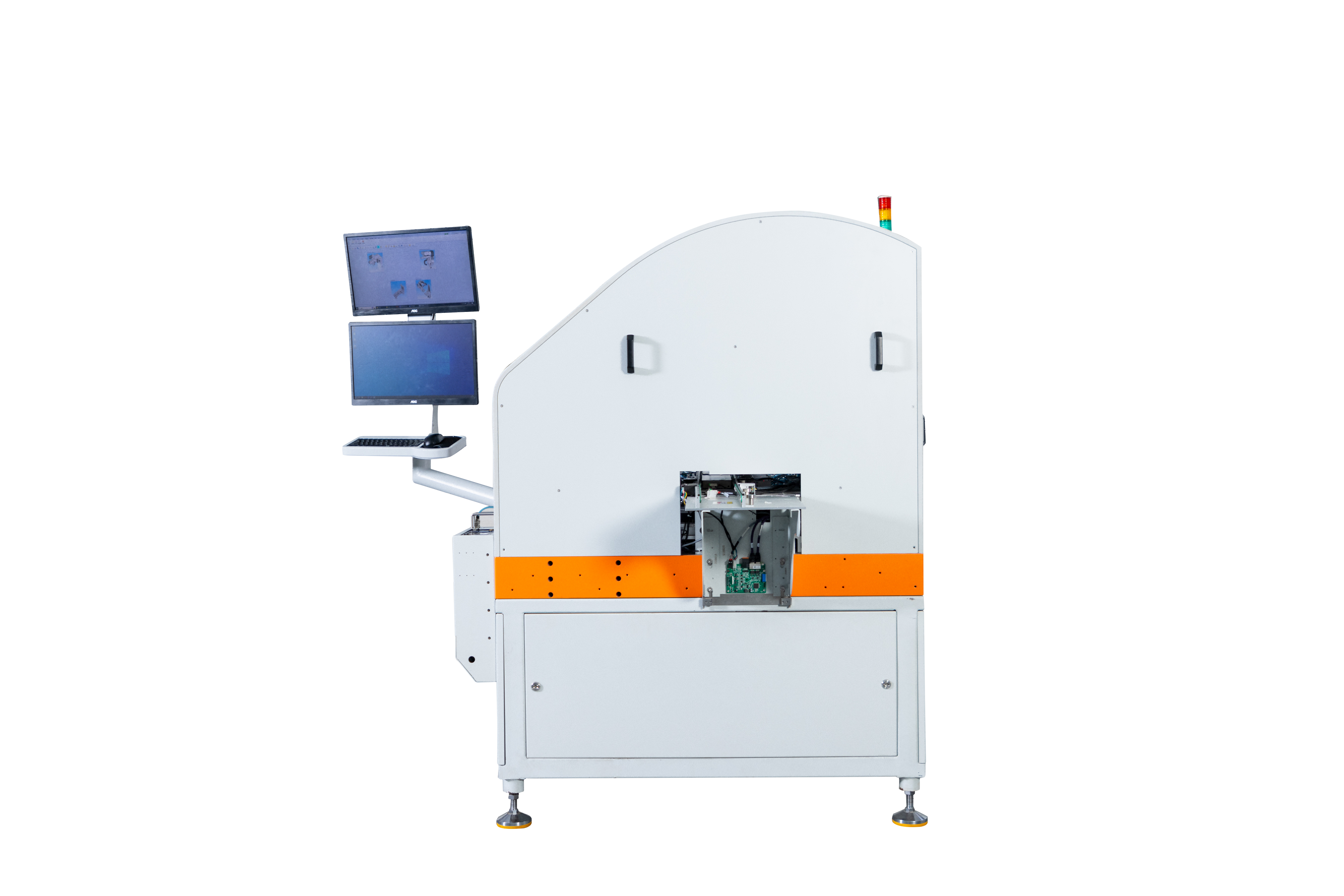
Side
Bond Head
Look-Up Camera
Wafer Stage
Ejector Pin