Brain-Computer Interface Sub-Micron Flexible Materials Eutectic SiP
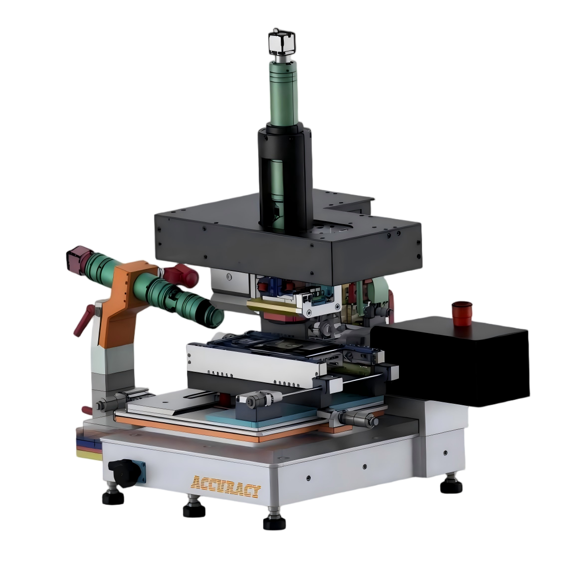
Qixin QX5000 Sub-Micron Advanced Interconnect
Advanced Packaging

Brain-Computer Interface Sub-Micron Advanced Interconnect

±0.5 μm
Placement Accuracy
0.1 N
Fine Force Control
Multi-Process
R&D Platform
Brain-Computer Interface Sub-Micron Advanced Interconnect

1. Micro-Assembly Target: What Are We Actually Assembling?

In January 2024, Elon Musk posted on X: "The first human patient has received a Neuralink implant and is recovering well." On screen, a completely paralyzed patient was controlling a computer cursor, typing, and even playing video games — using only their thoughts.

To date, 21 people worldwide have participated in Neuralink clinical trials. In early 2026, Musk further announced that Neuralink would begin mass production of BCI devices that year.

But behind the miracle of "thought-controlled typing" lies a critical engineering challenge rarely discussed — how do you precisely connect thousands of flexible electrodes, thinner than a human hair, onto a chip the size of a fingernail?

Below, we explore the emerging field of brain-computer interfaces (BCI) from a micro-assembly engineering perspective[1].

A typical implantable brain-computer interface (iBCI) system integrates a variety of technical components:

Table: Core Components of an Implantable BCI System

ComponentFunctionAssembly Challenge
CMOS ChipSignal acquisition, processing, wireless transmissionHigh-density I/O, sub-micron alignment
MEMS StructuresMicro-sensors, actuatorsCo-integration of precision mechanical structures and electrical interconnects
Flexible Electrode ArrayNeural tissue interface — recording or stimulating neural signalsUltra-thin flexible substrate, easily deformed, difficult to fix; requires "soft-to-hard" interconnect with rigid chips
Thin-Film SubstrateInterconnect routing carrierHeat-sensitive material, requires low-temperature processing
Biocompatible EncapsulationLong-term implant protectionHermeticity requirements, thermal management challenges

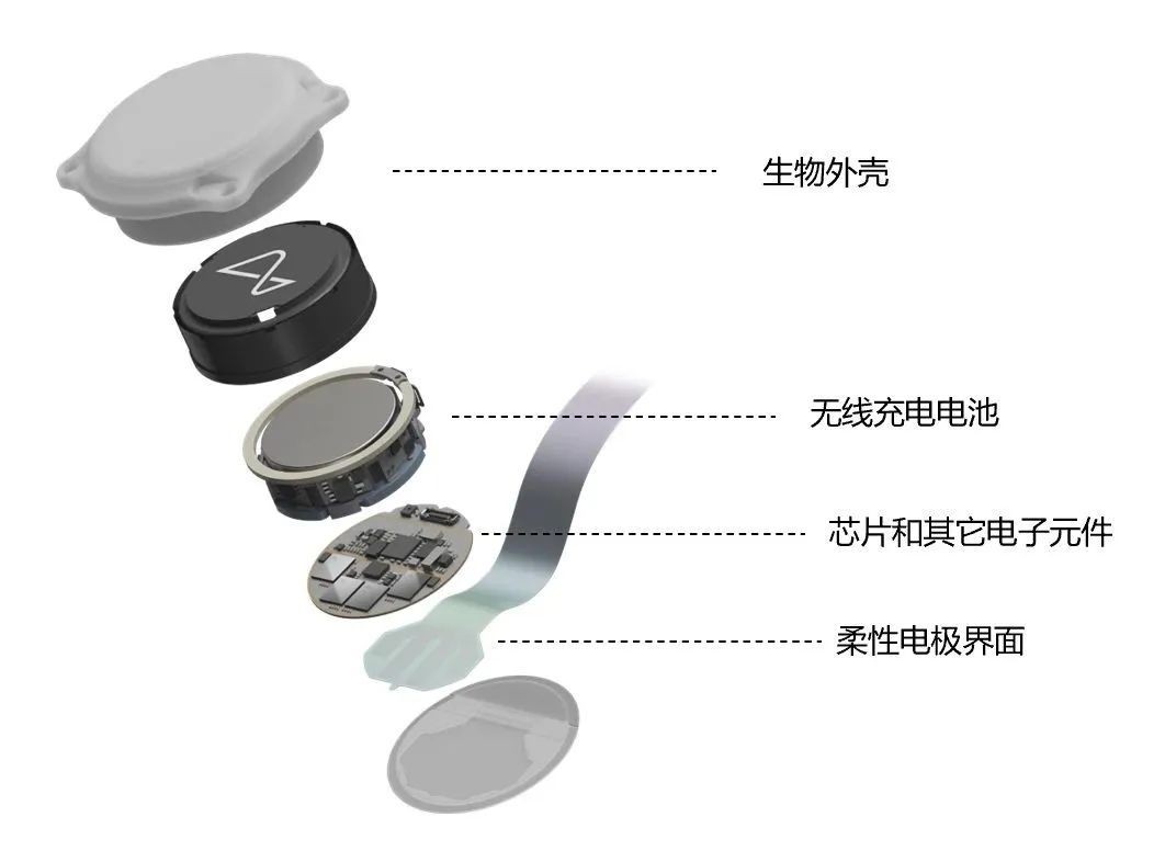
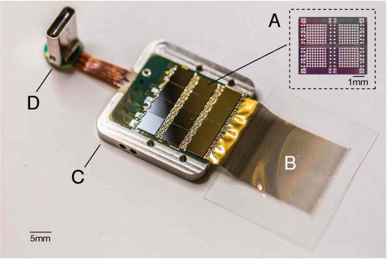
Neuralink BCI exploded view

▲ Neuralink BCI exploded view — multi-level interconnect structure of flexible electrodes and chips (Source: Neuralink)

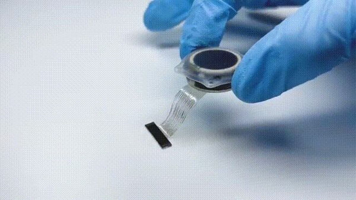
What are flexible electrodes? Simply put, electrodes are the "interface" between the brain and the machine — they capture neuronal electrical signals and relay them to the backend chip for processing. Traditional electrodes are typically rigid metal needles or probes that pierce or press against brain tissue, easily triggering immune reactions and inflammation.

Flexible electrodes solve this problem by using an ultra-thin polymer film as a substrate (thickness comparable to a human hair, approximately 1/10), densely packed with tiny electrode contacts that conform closely to the cerebral cortex and deform with tissue micro-movements. This "soft overcomes hard" design significantly reduces tissue damage and inflammation, allowing the implant to function stably in the brain for months or even years — a prerequisite for BCI to move from the lab to clinical application.
2. Three Engineering Challenges: Accuracy Is Only the Beginning

The introduction of flexible materials creates new engineering difficulties — how do you reliably connect such thin, easily deformable flexible electrodes to rigid chips? This is not just a material interface problem, but a convergence of three challenges: accuracy, force control, and thermal-power management.

Flexible electrode

▲ Flexible electrode — microelectrode contacts densely arranged on an ultra-thin polymer substrate

Challenge 1: Sub-Micron Alignment Accuracy

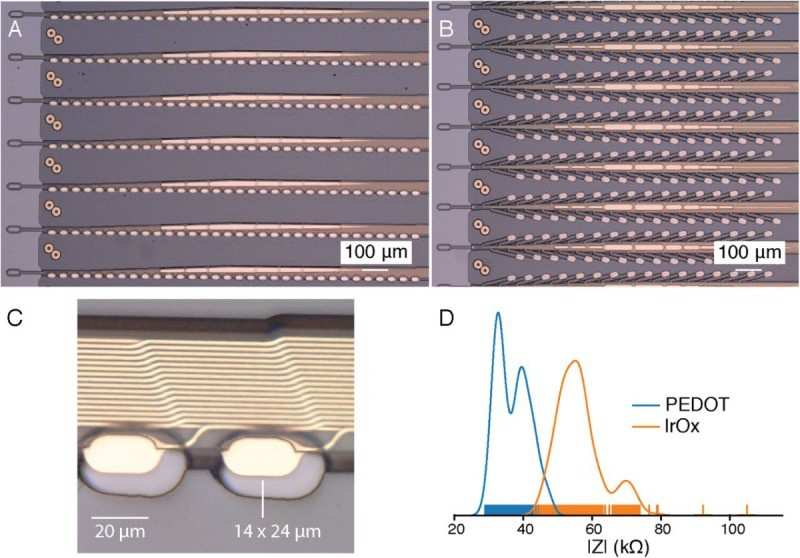
A typical high-throughput BCI chip requires thousands of micron-scale contacts to be precisely aligned: each Neuralink thin-film device features 3,072 electrode contacts, using flip-chip bonding to attach the integrated circuit to the electrode contacts in the thin-film sensor area, packaging 3,072 channels within an area of 23 × 18.5 mm²[3]. Stepper lithography can create metal films at sub-micron resolution, but flip-chip bonding onto these tiny contacts demands sub-micron placement accuracy — otherwise signal channels are lost.

Novel polymer probe flexible electrodes

▲ Novel polymer probe flexible electrodes with 50 μm and 75 μm contact spacing

Challenge 2: Biocompatible Flexible Materials and Interconnect Methods

BCIs use flexible electrodes precisely because their mechanical properties more closely match soft brain tissue, significantly reducing immune rejection and inflammatory response. However, the introduction of flexible materials brings new process challenges:

  • Force control challenge: Neuralink's flexible electrodes have a width comparable to a human hair, with thickness only about 1/10 of a hair. Too much bonding force crushes the electrode; too little results in poor contact and open circuits — "must press firmly but not crush," and this force window is extremely narrow.
  • Biocompatibility constraints: Fluxes, organic adhesives, and other materials commonly used in standard electronic packaging may cause toxic reactions or degradation failure in the body. Bonding materials must remain stable in bodily fluids long-term, and encapsulation must be hermetic to block fluid penetration. This means temporary adhesive fixation methods used in prototyping cannot carry over to the final product — the process path itself requires a "leap" from R&D to mass production.

In short: Flexibility solves tissue compatibility but creates chip connection difficulty.

Challenge 3: Thermal and Power Management

Implants directly contact brain tissue and face extremely strict thermal budgets — even a 1°C temperature rise can cause irreversible neural damage.

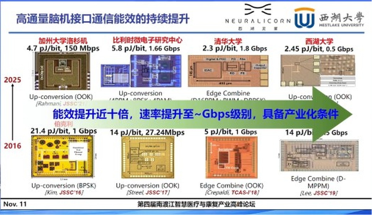
Higher power means more heat, forcing chip power consumption to ultra-low levels: Neuralink's single-chip power is only 6 mW, and Samsung's use of 4 nm process technology for its next-generation chip is driven primarily by energy efficiency considerations. Yet high-throughput recording (thousands of channels in parallel) and wireless data transmission continuously consume power — 60% of power is consumed by data transmission. While the academic community has improved communication energy efficiency nearly 10-fold over the past decade and boosted data rates to Gbps levels, the conflict between power and performance remains far from resolved.

This contradiction places higher demands on chip interconnect methods and integration density — shorter interconnect paths mean lower transmission power, while higher integration requires connecting more channels in a smaller area, both pointing toward high-density, short-interconnect advanced packaging solutions.

3. Three Challenges Overview

Three Challenges at a Glance: Accuracy determines whether alignment is possible → Flexibility determines stability in the body → Thermal & power management determines safety and longevity.

Facing these challenges, the global academic and industrial communities are pursuing a dual-track approach: improving chip energy efficiency and integration on one side, while breaking through micro-assembly process bottlenecks on the other.

BCI energy efficiency improvement

▲ Continuous improvement in BCI energy efficiency is the foundation for industrialization

4. From Lab to Clinic: Domestic and International Progress

Taking implantable BCIs as an example, overseas development is led by Neuralink. As of 2025, Neuralink has completed a cumulative 21 human implantations. Samsung Electronics has secured the order for Neuralink's fourth-generation brain implant chip, using a 4 nm process, internally codenamed "O1," targeting mass production in 2027.

On the domestic front, China's independent BCI R&D is progressing from multi-point breakthroughs toward industrialization: On June 1, 2026, China's National Medical Products Administration (NMPA) officially approved the clinical trial application for the world's first invasive BCI chip — a landmark decision that could give China an early advantage in the BCI race[4].

Table: Key Domestic BCI Institutions and Progress

InstitutionStage / RoleAchievements
Westlake Lingxi Technology
(Incubated by Westlake University)
Chip design → industrialization phaseSelf-developed 40 nm BCI chip, 256-channel tape-out verified, 1024-channel chip architecture showcased at ISSCC 2026; targeting Chinese-language neural prosthesis, system latency < 10 ms, decoding ~30 Chinese characters per minute; selected for MIIT "Open Competition" program 2025; completed tens of millions RMB Angel+ funding round in June 2026[2]
Neurohope Technology
(Shanghai)
Invasive product approved → commercializationWorld's first invasive BCI medical device NEO-ONE SCI approved for market in March 2026; as of June 2026, 36 implant surgeries completed, cumulative safe implant days exceeding 14,000, 68.8% of patients showing significant manual function improvement 6 months post-surgery; STAR Market IPO accepted, proposed fundraising of RMB 2.5 billion, aiming to become "BCI First Stock"
NeuroTiger Technology
(Shanghai)
Entered Class III medical device registration clinical stageFully implantable, fully wireless, fully functional BCI system officially launched GCP registration clinical trial at Huashan Hospital in July 2026, the first domestic subdural surface-implantable BCI product to enter national Class III medical device registration clinical trials; collaborating with 15 Grade-A hospitals in multi-center study; Jiangxi "Super Factory" with planned area of 14,300 m² targeting mass production in H2 2026, achieving 10,000-unit stable delivery capacity

These developments show that BCI is moving from "lab-feasible" to "repeatably manufacturable." And this leap cannot happen without the support of precision bonding technology.

5. Equipment Support: From "Connecting Electrodes" to "Building the Entire Micro-System"

The "miniaturization" of BCI means making the entire system small — fitting electrodes, chips, wireless modules, and power management into a coin-sized implant. This involves three levels of interconnect challenges:

Table: Three Interconnect Levels of BCI Miniaturization

Interconnect LevelCore RequirementKey Process
Level 1: Chip ↔ Electrode
(Front-end acquisition)
Connecting thousands of contacts on flexible electrodes one-to-one with ASIC chip padsSub-micron flip-chip bonding
Level 2: Multi-Chip System Integration
(Processing & communication)
Interconnecting multiple chips (ASIC, power management, wireless communication) within a tiny implantSystem-in-Package (SiP), heterogeneous integration
Level 3: Implant Encapsulation
(Long-term reliability)
Hermetic sealing of the entire module to ensure years of stable operation in the bodyThermal management, stress control, material compatibility

The three levels correspond to chip flip-chip bonding, system-in-package, and hermetic sealing, each independent yet interdependent. This means micro-assembly equipment must simultaneously meet requirements for accuracy, force control, thermal management, and process flexibility.

Process Evolution: From Adhesives to Eutectic

In BCI development, early prototyping stages often use temporary adhesive fixation for chips, quickly establishing functional verification — low cost, fast iteration. However, adhesive bonding is unsuitable for human implantation environments; the final solution must transition to biocompatible bonding (such as flux-free eutectic soldering).

This means that in the implantable medical device field, the process choices made during early R&D are often not the final answer; equipment must have sufficient flexibility to accommodate mid-course changes. This imposes clear "process upgradeability" requirements on bonding equipment:

  • A single platform covering multiple bonding methods: adhesive, eutectic soldering, ultrasonic bonding, etc.
  • Switching between bonding methods without replacing the entire machine or significantly adjusting hardware
  • Heating modules, pick-and-place tools, etc. customizable for different bonding methods

6. QX5000: Ready for BCI Precision Interconnect

Facing the three challenges and process evolution demands of BCI micro-assembly, the QX5000 multi-purpose sub-micron die bonder provides system-level support for BCI precision interconnect:

Table: QX5000 Capabilities vs. BCI Requirements

Interconnect LevelCore RequirementQX5000 Capability
Chip ↔ Electrode±0.5 μm alignment accuracy, ultra-low force control±0.5 μm placement accuracy, 0.1 N fine force control
Chip ↔ ChipMulti-chip SiP integration, high-density interconnectSupports multi-chip placement, stacking, CoG/CoF processes
Package ↔ ReliabilityPrecise temperature control, atmosphere protection, stress control450°C ± 1°C temperature control, N₂/formic acid protection, < 0.5 μm/25 mm coplanarity

With over a decade of engineering and process expertise in optical communications, infrared imaging, MEMS, and other fields, Accuracy has developed a mature process methodology in sub-micron alignment, ultra-low force control, and multi-material compatibility, and can provide cleanroom environments for process validation. The QX5000's modular architecture and configurable process units are purpose-built for application scenarios of "iterate during development, validate during iteration."

Neural interface designs evolve rapidly, material combinations continuously change, and assembly processes must adapt throughout development. Equipment must be prepared for scenarios of "iterate during development, validate during iteration" while paving the way for future scaled production.

If you are evaluating micro-assembly processes for BCI-related applications, please contact us to learn more about QX5000's process capabilities in this field, and schedule an on-site visit and process trial at any time.

±0.5 μm Accuracy 0.1 N Force Control 450°C ± 1°C Heating
艾科瑞思

Suzhou Accuracy Intelligent Equipment Co., Ltd., founded in 2010 and headquartered in Suzhou Industrial Park, is a professional supplier of high-precision advanced semiconductor packaging equipment, dedicated to the research, design, manufacture, and sale of high-accuracy, high-throughput, high-reliability, and intelligent die bonding systems.

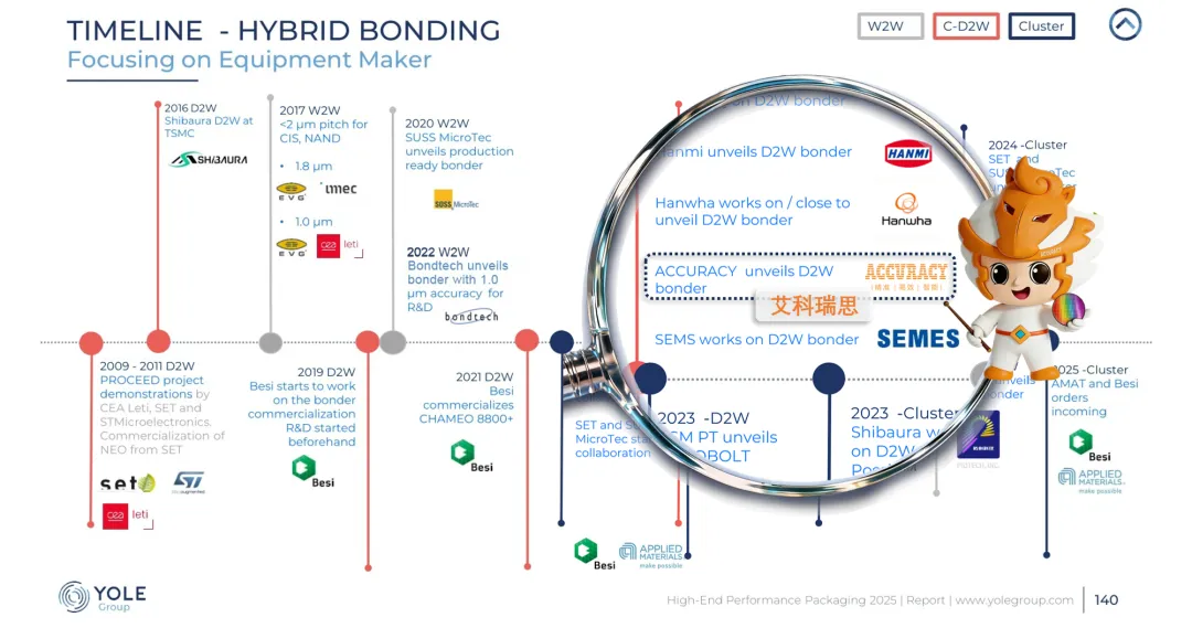
With 16 years of deep industry experience, Accuracy provides next-generation die bonding equipment for emerging semiconductor materials and advanced packaging processes — including multi-chip die bonders for system-in-package (SiP), die sorters, wafer-level hybrid bonders (Chip-to-Wafer Hybrid Bonder with 200 nm alignment accuracy, becoming the first Chinese D2W equipment supplier recognized in the Yole Group 2025 report; project fully divested), and flip chip bonders — serving customers across advanced packaging, IC assembly, RF/microwave, optoelectronics, and sensor markets with professional die bonding solutions.

艾科瑞思
References
  • [1]Finetech GmbH. How Implantable Brain-Computer Interfaces Are Pushing the Boundaries of Precision Die Bonding[EB/OL]. 2026.
  • [2]Zhang Y Q. Yang Jie of Lingxi Technology: Invasive BCIs Moving Toward High-Throughput, Fully Implantable[N]. iJiwei, 2025-11-11.
  • [3]Musk E, Neuralink. An integrated brain-machine interface platform with thousands of channels[J]. bioRxiv, 2019.
  • [4]China Electronics News. Three Questions on BCI Chips[EB/OL]. 2025-07-11.