Three Core Bonding Challenges on Large Panels
The customer is a panel-level packaging and test manufacturer running System-in-Package (SiP) multi-chip bonding. Substrate size is 330×330 mm with significant incoming warpage. The product line covers three adhesive routes—epoxy dispensing, DAF (Die Attach Film), and sintered silver—and all DAF-type products require bonding under a heated substrate condition.
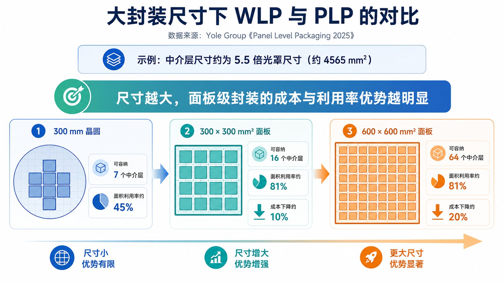
Panel-level packaging replaces the round wafer carrier with a square panel: higher area utilization and lower per-die cost—but the engineering challenges of a large substrate go far beyond "a bigger board." The following are the application challenges of large-substrate / panel-level DAF heated bonding.
Table: Challenges in panel-level / large-substrate multi-chip DAF heated bonding
| Challenge | Quantified Description | Industry Status |
|---|---|---|
| Thermal warpage instability | 330×330 mm substrate, mm-level warpage; DAF heating at 200°C → combined deformation | Large-panel bonding warpage is the core bottleneck of PLP volume production (Yole 2025) |
| Multi-process window development | Dispensing / DAF / sintered silver routes, each with distinct force-temperature-time windows | Each material changeover means re-validation of tooling + recipe + calibration |
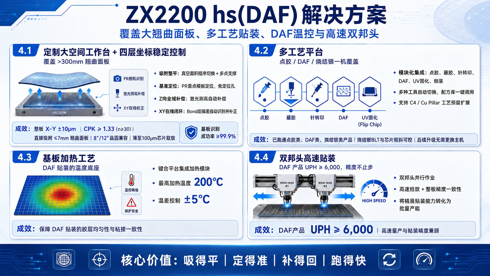
| Panel-wide accuracy consistency | ±10μm at CPK≥1.33; edge-vs-center deviation varies point by point | Single-point accuracy ≠ panel-wide consistency; accuracy and throughput together are the acceptance gate |
These three pain points are interconnected—thermal warpage affects chuck holding and alignment reference, the multi-process window determines changeover efficiency and uptime, and panel-wide consistency is the acceptance gate where accuracy and throughput must hold simultaneously. Improving a single dimension is not enough; intervention is needed simultaneously across four dimensions: thermal field, chuck holding & leveling, process platform, and accuracy closed-loop.