Indium Flip-Chip Bonding Interconnection — The Interconnection Evolution of Superconducting Quantum Chips from Planar to 3D
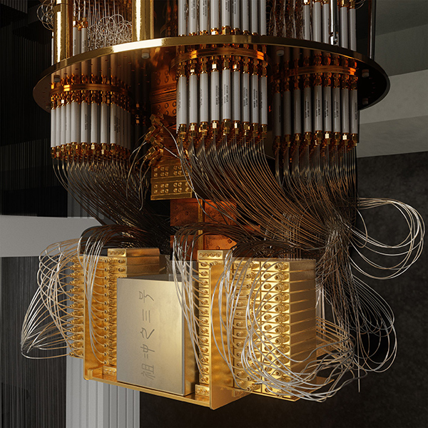
Quantum computing has become a primary arena of national technological competition. On March 3, 2025, the University of Science and Technology of China (USTC) announced Zuchongzhi-3, a 105-qubit superconducting quantum computing prototype, which outperforms the fastest supercomputer by fifteen orders of magnitude on specific problems. In 2026, quantum technology was written into the government work report and the highest-priority list of the 15th Five-Year Plan, and the national will is pushing this field even deeper.
I、What Makes Quantum Computers Powerful?
A quantum computer is a computer that uses quantum mechanics to perform certain computations more efficiently than classical computers.
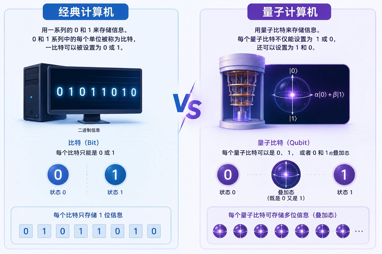
A quantum computer not only has strong storage capability but also remarkable parallel computing power. A classical computer computes one possibility at a time, while a quantum computer computes all possibilities at once — like light passing through every slit in a wall simultaneously.
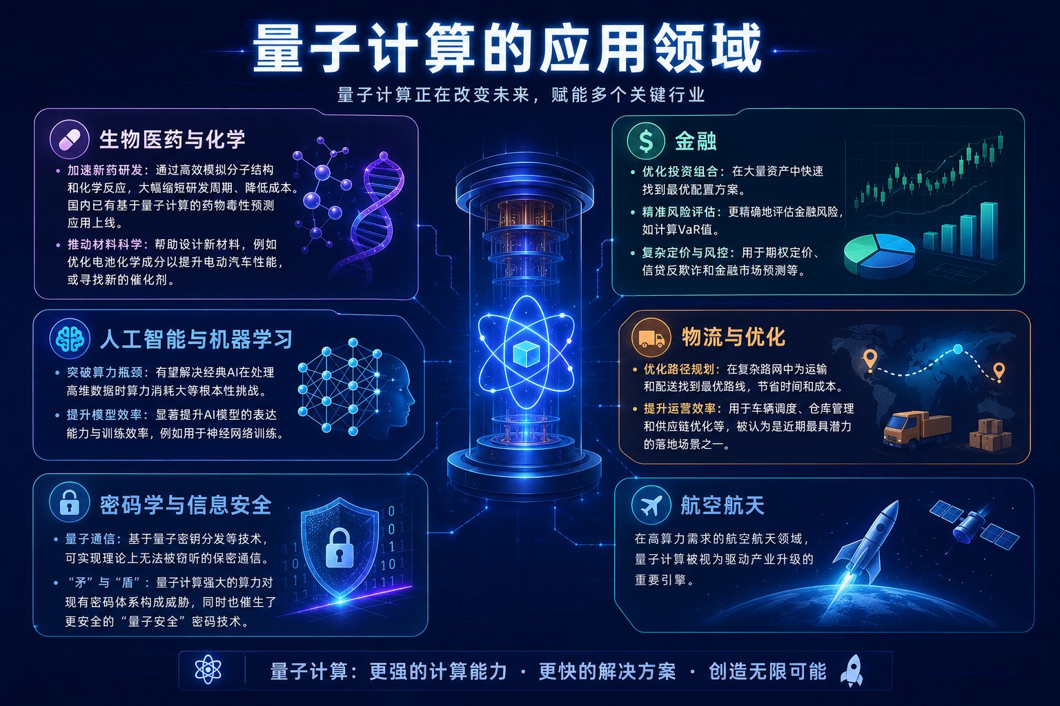
Meanwhile, advances in quantum computing will empower artificial intelligence, reducing errors in AI applications and creating intelligent systems that enable early diagnosis of problems.
II、How Advanced Interconnection Empowers Quantum Computing?
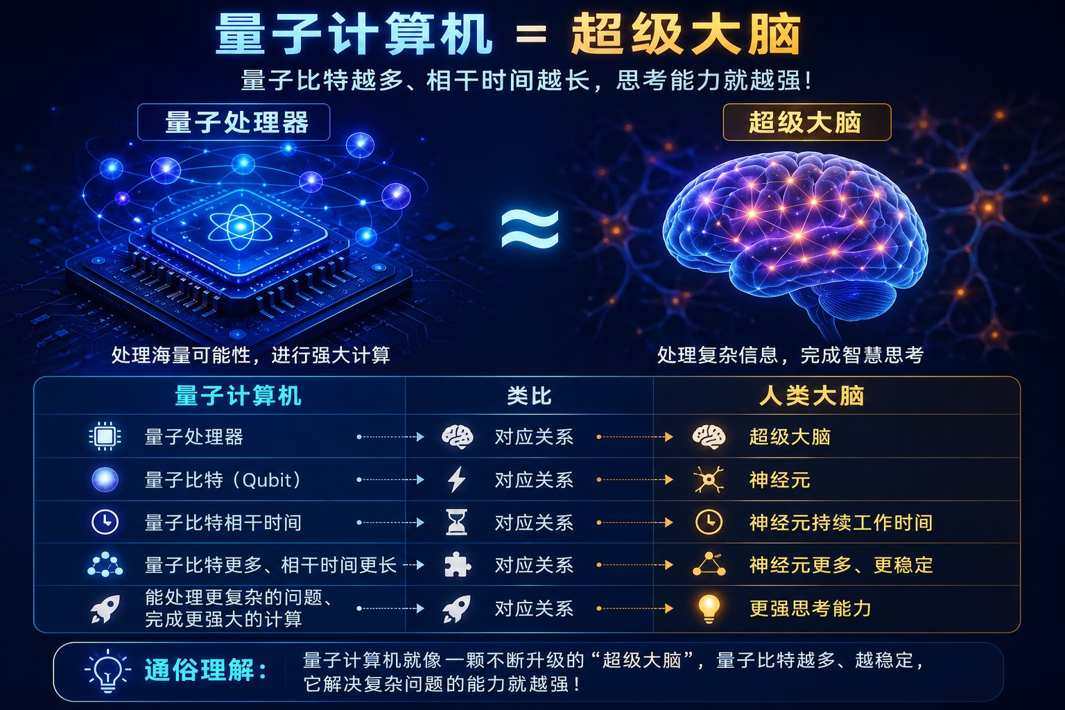
Professor Zhu Xiaobo of USTC once used an analogy: 'A quantum processor is like a super brain, qubits are the neurons, and qubit coherence time can be understood as the time neurons can work effectively. The more qubits and the longer the decoherence time, the more complex and massive the information the brain can process, and thus the more difficult problems it can solve.'
A computationally useful, fault-tolerant quantum computer with error correction requires roughly tens to millions of physical qubits to build sufficient logical qubits (over 1000), and each qubit must be individually controlled, read out, and coupled to others — which requires massive wiring to transmit signals between external classical processors and internal qubits.
The real challenge is making more qubits and connecting them more densely — and that is exactly the battlefield of packaging interconnection.
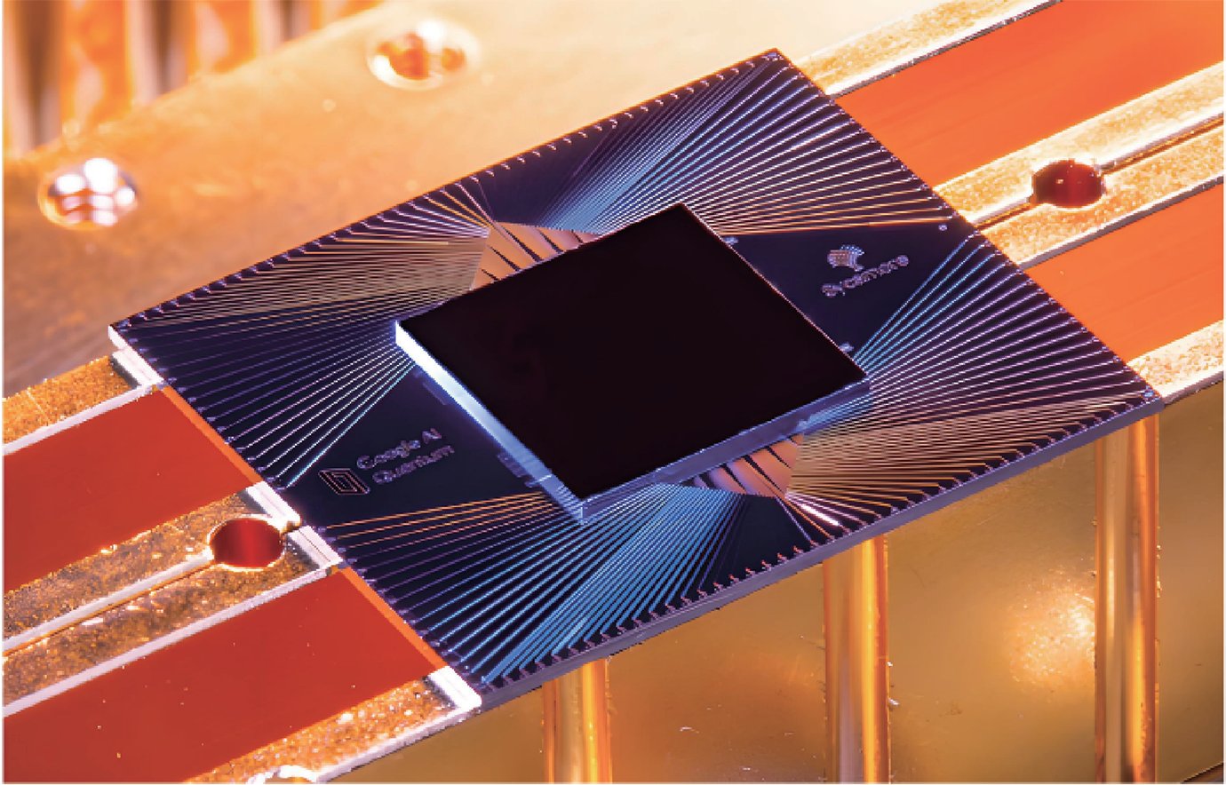
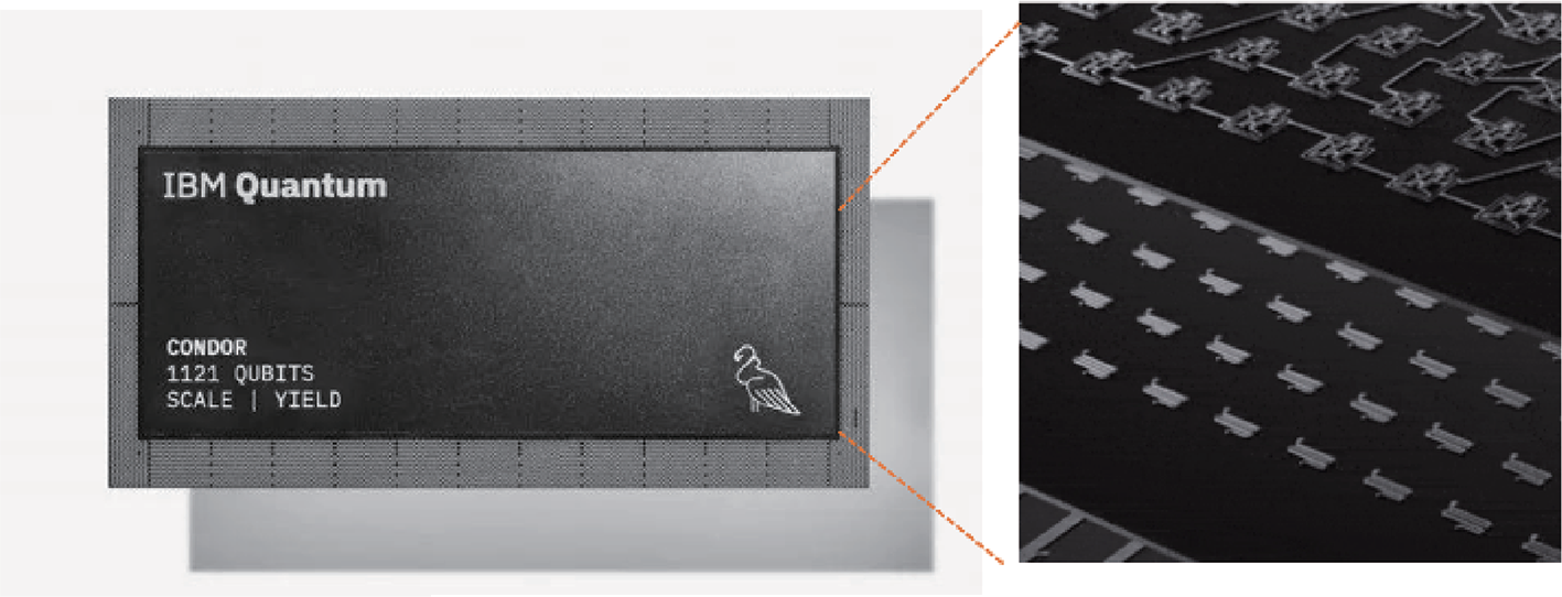
Why must we stack? Traditional 2D planar layouts encounter severe signal wiring congestion and crosstalk once qubit count exceeds roughly 50. Similar to the packaging evolution of classical silicon CMOS chips, as quantum chips grow in compute power and qubit count, the packaging architecture of superconducting quantum chips is shifting from planar single-chip design toward Flip-chip interconnect, and further exploring TSV-based 3D integration.
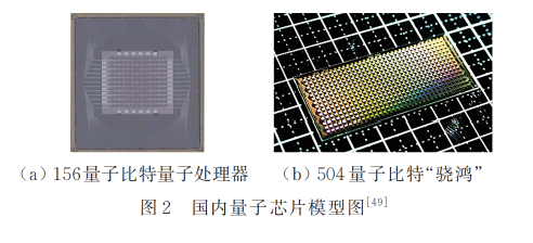
Domestic quantum computing chips are also thriving. In recent years, USTC, the Beijing Academy of Quantum Information Sciences, and the CAS Innovation Academy for Quantum Information have achieved excellent results in superconducting quantum computing. Especially in the past two years, processor qubit counts have leapt from tens to hundreds, evolving from planar 'Flip-chip' technology toward higher-level stacking.
III、Integration Challenges and Process Implementation of Superconducting Quantum Chips
There are multiple technological routes to quantum computers, and given their different advantageous scenarios, multiple routes may coexist in the future. Among them, the superconducting system — compatible with semiconductor micro-nano processes and most scalable — is one of the most mature mainstream approaches for engineering.
Superconducting quantum computing is a technology that uses the macroscopic quantum effects of superconducting materials at extremely low temperatures for information processing.
In the integration of superconducting quantum chips, the following challenges are faced:
Challenge 1 · Superconducting materials and physical compatibility in extreme environments — able to withstand temperatures colder than outer space
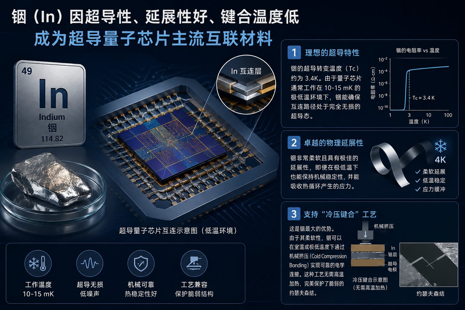
Quantum packaging cannot use copper, lead, or tin bonding like traditional semiconductors — it must remain superconducting at cryogenic temperatures, while the bonding temperature cannot be too high to avoid damaging fragile structures.
Indium (In) has become the mainstream interconnect material for superconducting quantum chips due to its superconductivity (Tc≈3.4K), good ductility, and low bonding temperature.
Challenge 2 · Under the requirement of maintaining superconducting quantum properties, interconnection must be low-loss, highly reliable, and scalable
Impurity defects at chip interfaces (TLS) 'steal' the energy of qubits. To preserve performance, qubits must operate 'suspended' facing air or vacuum — which directly disables traditional Underfill, leaving the package inherently fragile. The special superconducting material system and qubit scaling also introduce new packaging issues: thermal cycling stress, spurious resonances of large chips, and crosstalk.
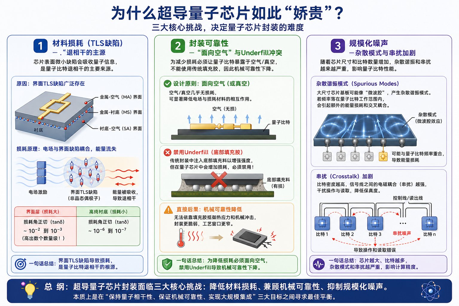
Challenge 3 · Process challenges of indium bump interconnect — it 'eats' aluminum and 'collapses'
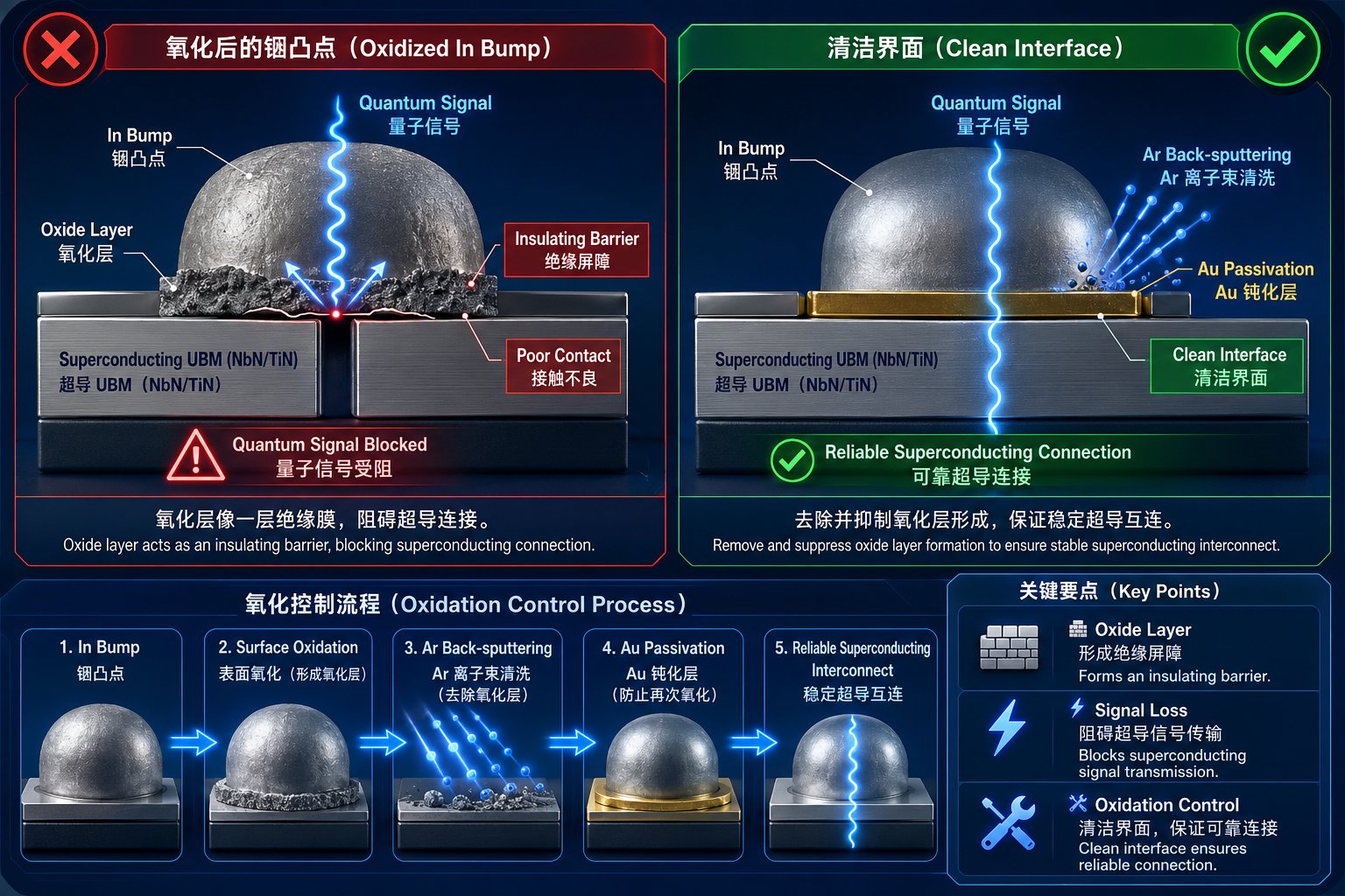
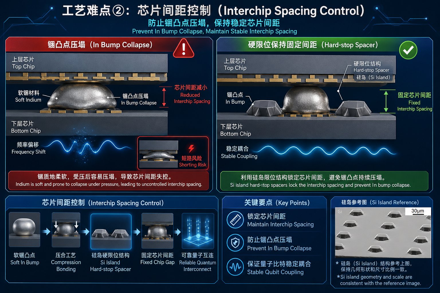
Indium bump interconnect faces two major problems in 3D stacking of superconducting quantum chips:
First, mutual diffusion between indium and the aluminum wiring layer forms non-superconducting intermetallics and readily produces oxides, degrading signal connections.
Second, repeated bonding causes progressive collapse of the soft indium bumps, making it hard to maintain stable gaps and easily damaging the chips.
Both must be solved under the stringent low-temperature, low-loss constraints above.
Indium Flip-Chip Bonding Applications for Superconducting Quantum Chips
Source: LI H X. Flip-chip integrated superconducting quantum processors[D]. Göteborg, Sweden: Chalmers University of Technology, 2025.
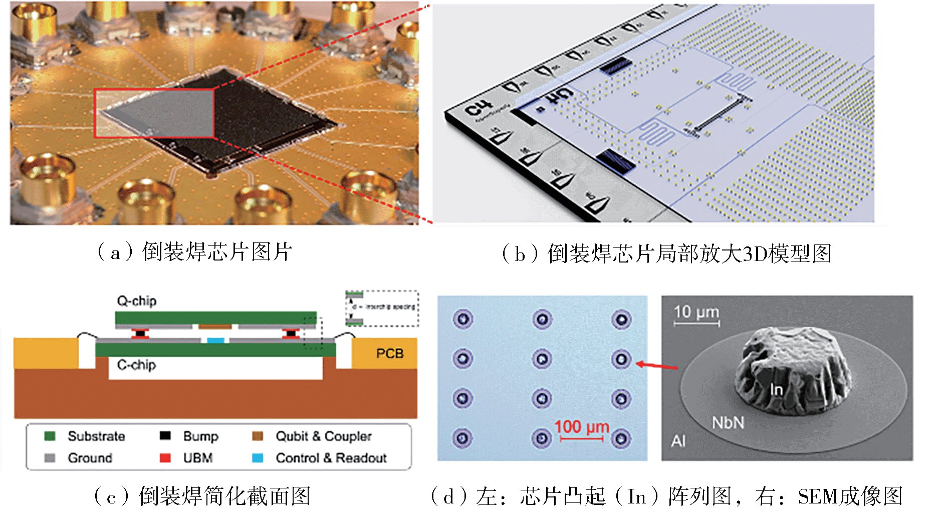
| Bonded objects | Qubit chip (Q-chip, carrying qubits and couplers) and control chip (C-chip, carrying control lines, readout lines, and resonators) |
|---|---|
| Q-chip size | ~12 mm × 12 mm |
| Chip spacing | target ~8 μm |
| Bump scheme | Indium (In) bumps + superconducting UBM layer (NbN, as diffusion barrier against In-Al inter-diffusion), Al-NbN-In structure |
| Bonding process | Room-temperature cold compression — after flipping the Q-chip and precisely aligning it with the C-chip, cold compression is completed at room temperature by mechanical pressure, with no reflow and no ultrasound |
| Validation result | Successfully implemented a 25-qubit-scale superconducting quantum processor; qubit coherence times (T1, T2*) and gate fidelity under the flip-chip architecture are comparable to the monolithic architecture, with no degradation from the added process steps |
The QX5000 provides a customized R&D platform for qubits moving toward large-scale 3D integration.
Solution
As superconducting quantum chips scale from tens to hundreds of qubits, the packaging architecture must move from planar to 3D stacking, and flip-chip bonding becomes the key path to break through the I/O bottleneck. Around the core indium flip-chip bonding process for superconducting quantum, the QX series provides professional solutions:
- Sub-micron alignment accuracy — ±0.5μm alignment accuracy, covering the ±1–2 μm window required for superconducting qubit interconnects, with ample margin for scaled integration.
- Redox — the equipment can be configured with a formic-acid chamber for in-situ cleaning before bonding, ensuring a clean interface and low-resistance superconducting connection.
- Pick-and-place and bonding control — for chip warpage and bump layout variations, customized nozzles and process libraries are provided to ensure stable pickup and coplanar placement, suppressing uneven collapse at the source.
- Cold / thermo-compression compatible — supports both cold and thermo-compression modes, adapting to different material process systems.
- Gap control — 0.1 N force-control accuracy with real-time closed-loop force control precisely regulates bump collapse and chip spacing, avoiding over-pressure collapse and under-pressure voids, stabilizing the inter-chip gap within the process window.
Take superconducting flip-chip interconnection from paper to production
The Qixin QX5000 already supports the full indium flip-chip bonding process validation. Share your chip specs and integration requirements, and our process team will arrange sample bonding and parameter matching for you.
Book a Process Trial →Accuracy (Suzhou Accuracy Intelligent Equipment Co., Ltd.), founded in 2010 and headquartered in Suzhou Industrial Park, is a specialized supplier of high-precision advanced semiconductor packaging equipment, focused on the R&D, design, manufacturing and sales of high-precision, high-speed, high-reliability and intelligent die-bonding systems.
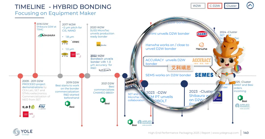
After 16 years of industry dedication, Accuracy provides a new generation of die-bonding equipment for emerging semiconductor materials and advanced packaging processes — including System-in-Package (SiP) multi-chip die bonders, sorters, wafer-level hybrid bonders (Chip-to-Wafer Hybrid Bonder, alignment accuracy 200 nm, becoming China's first D2W equipment supplier listed in the Yole Group 2025 report) and flip-chip die bonders — serving professional die-bonding solutions for advanced packaging, IC assembly, RF/microwave, optoelectronics and sensor markets.
Some images and data on this page are cited from public academic literature and public reports, for popular-science purposes only.
References
- LUAN T, LIU X, DAI Z, et al. Progress in integrated process technology for superconducting quantum processors[J]. Microelectronics, 2025, 55(3): 430-440.
- LI H X. Flip-chip integrated superconducting quantum processors[D]. Göteborg, Sweden: Chalmers University of Technology, 2025.
- LUO Z, MAYER T, ZAHN D, et al. A demonstration of multifloating superconducting qubits on a 3-D flip-chip platform with TLS loss mitigation via apertures[J]. IEEE Microwave and Wireless Technology Letters, 2025, 99: 1-4.
- PARADKAR A, NICAISE P, DAKROURY K, et al. Superconducting flip-chip devices using indium microspheres on Au-passivated Nb or NbN as under-bump metallization layer[J]. Applied Physics Letters, 2025, 126(2): 022601.
- PEZESHKI K, GUAN H. Flip-chip indium bump bonding for superconducting circuit integration[R]. Stanford, CA: Stanford Nanofabrication Facility (SNF), ENGR 241 SPR23 Final Report, 2023.
- Structure Analysis of 3D Integrated Superconducting Quantum Chips[R]. San Jose, CA: San Jose State University, 2025.
