MicroLED Heterogeneous Bonding Flip-Chip Photonics
Qixin QX5000 Multi-Purpose Sub-Micron Die Bonder | MicroLED Heterogeneous Bonding Process Development Platform
Photonics

MicroLED Heterogeneous Bonding Solution — QX5000 Sub-Micron Bonding Validation Support

±0.5μm
Standard-die Placement Accuracy
Flip / Back Bond
Multi-Process Platform
0.1–30N
Full-Range Force Control
MicroLED Heterogeneous Bonding Solution — QX5000 Sub-Micron Bonding Validation Support

MicroLED: From Chip Assembly to Wafer Integration

MicroLED is hailed as the ultimate solution for next-generation displays — offering higher brightness, better energy efficiency, and longer lifespan than OLED. If we compare MicroLED industrialization to a long-distance race, the bottleneck has shifted from 'chip manufacturing' to 'efficient assembly.' Traditional pick-and-place assembly, constrained by accuracy and throughput, can no longer meet high-density integration demands — especially in AR/VR silicon-based microdisplays (LEDoS), where assembling millions of pixels poses entirely new process challenges.
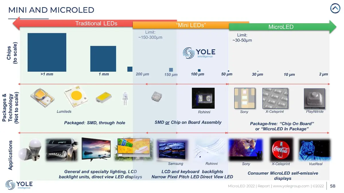
LED to MicroLED chip size shrink
▲ Current mainstream MicroLED chip sizes range from 20–50 μm, with the industry pushing toward 10 μm and laboratories exploring the 2–5 μm range

The core of MicroLED assembly is the precision interconnect of two heterogeneous materials:

First, the GaN (gallium nitride) epitaxial emissive layer, providing high-brightness self-emissive units;

Second, the silicon-based CMOS driver circuit, responsible for pixel-level independent driving and high-speed signal control.

Advanced packaging technology plays a critical role here, fusing 'emissive material' with 'logic computation' into one — this is heterogeneous integration.

This is fundamentally different from traditional LED assembly. Traditional LEDs typically mount tens to hundreds of chips onto a PCB or bracket via pick-and-place equipment; the chips are large (usually >200 μm), alignment tolerance is loose, and the process is mature and cost-controllable. But MicroLED pixel pitch has shrunk from hundreds of microns in early days to tens of microns, with a single chip only one-tenth the size of a traditional LED or smaller; each display must transfer millions to tens of millions of chips — the traditional 'mover' style of physical pick-and-place has hit its ceiling in both throughput and accuracy.

Thus MicroLED must leverage semiconductor process technology to achieve heterogeneous integration, shifting from physical handling to wafer-level or chip-level micro/nano fabrication.
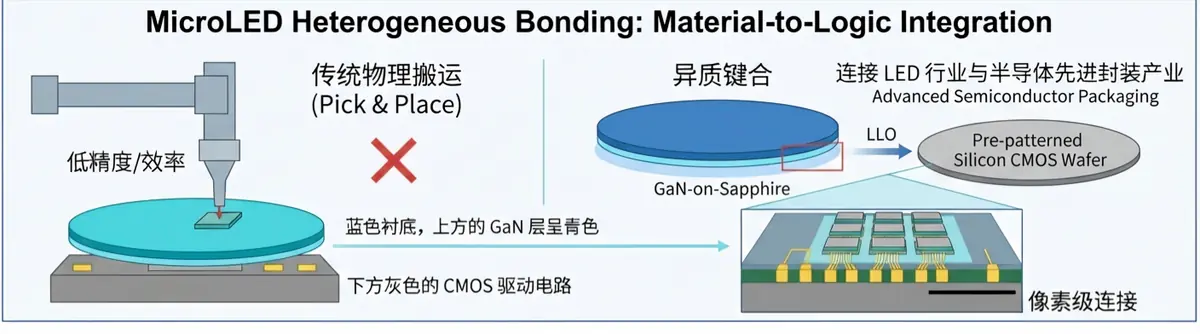
MicroLED heterogeneous integration: from physical handling to wafer-level fabrication
▲ MicroLED heterogeneous integration: from physical handling to wafer-level micro/nano fabrication

'Semiconductor heterogeneous integrated circuits are integrated circuits or systems realized by integrating high-performance compound-semiconductor devices or chips, silicon-based low-cost high-integration devices (including optoelectronic devices or chips) and passive components (including MEMS) or antennas from different process nodes via heterogeneous bonding or epitaxial growth.' — Academician Mao Junfa, Chinese Academy of Sciences [1]

Yet this 'marriage of materials' is far from easy — the emissive material (GaN) and the driver circuit (silicon) come from entirely different material systems, giving rise to a series of engineering challenges.
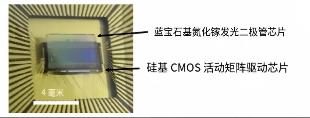
MicroLED: From Chip Assembly to Wafer Integration ▲ Emissive array (GaN) flip-chip bonded to CMOS driver circuit, achieving pixel-level electrical connection

Engineering Challenges of MicroLED Heterogeneous Bonding

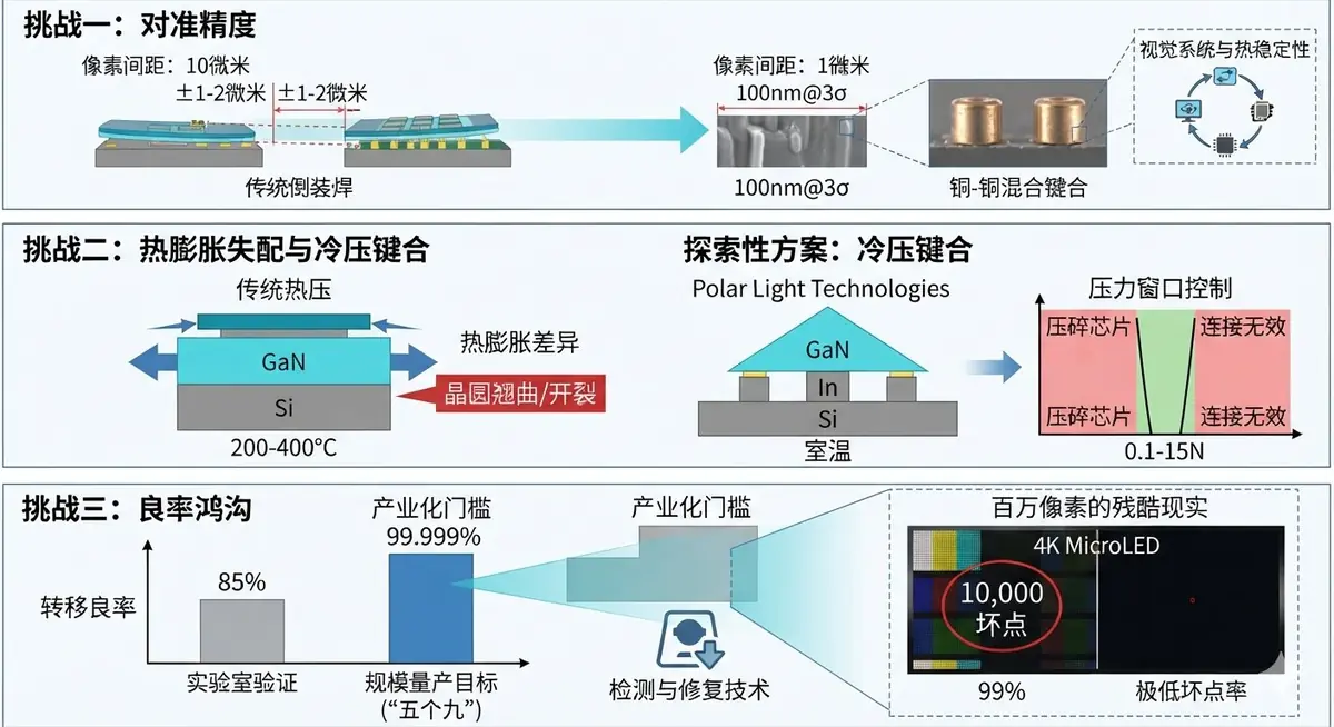
Challenge 1: Alignment Accuracy — Smaller Pixels, Narrower Tolerance

MicroLED pixel pitch has continuously shrunk from tens of microns in its early days. The larger the pitch, the wider the alignment tolerance; the smaller the pitch, the accuracy requirement rises exponentially. The industry currently targets 10 μm pitch as the main challenge; at this scale, flip-chip bonding — where the chip is flipped and bonded directly to the substrate pad via metal bumps or solder — requires alignment accuracy within ±1–2 μm. As pitch pushes below 5 μm and ultimately toward the 1 μm limit, alignment accuracy must cross into the semiconductor-grade 100nm@3σ range.

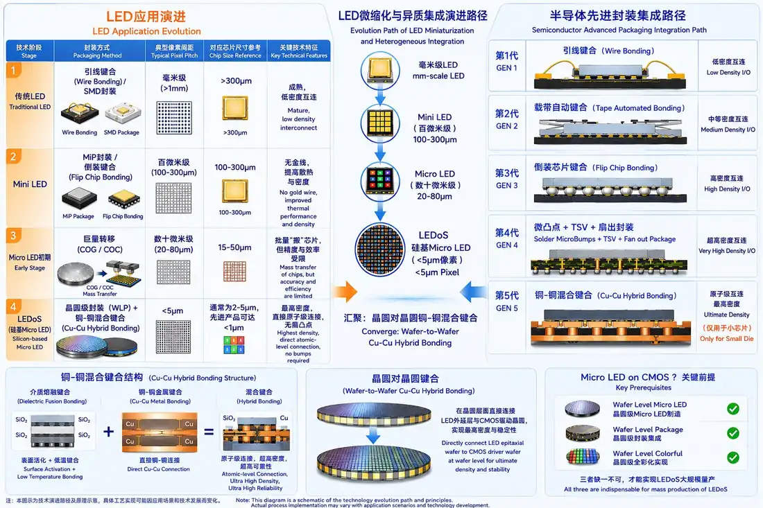
Evolution of LED applications and advanced packaging integration methods
▲ Evolution of LED applications and advanced packaging integration methods (Source: Yole [3])

Challenge 2: Thermal Expansion Mismatch — How to Bond Without Heating?

Whether sapphire or silicon carbide substrates, there is significant CTE (coefficient of thermal expansion) mismatch with silicon. Traditional thermocompression bonding requires heating to 200–400°C; within this temperature range the two materials expand differently, generating huge residual stress upon cooling, leading to wafer-level warpage or even chip cracking. Notably, GaN-on-Si, due to its material homology with the CMOS driver circuit, is becoming one of the mainstream directions to reduce CTE mismatch risk.

One exploratory approach is cold compression bonding: at room or low temperature, plastic deformation bonding of metal pads (e.g., indium) is achieved through precisely controlled pressure, with no heating or only slight warming throughout. Polar Light Technologies adopted this approach in its MicroLED microdisplay development, room-temperature pressing GaN pyramid chips onto indium pads on the silicon substrate, achieving an initial transfer yield of 85% [2].

Three major challenges of MicroLED heterogeneous bonding
▲ Three major challenges of MicroLED heterogeneous bonding: alignment accuracy, thermal expansion mismatch, yield gap

Challenge 3: From 85% to 99.999% — The Yield Gap

An initial yield of 85% is a significant breakthrough at the lab validation stage, but for a microdisplay with millions of pixels, a 15% defect rate means the entire device is unusable. The industry widely agrees that MicroLED mass production requires a single-transfer yield of 99.999% ('five nines') [2].

From 85% to 99.999% — not a linear improvement, but a leap across orders of magnitude. Each percentage-point gain involves systematic iteration of dozens of process parameters including bond force curve optimization, pad morphology control, surface cleaning, and alignment compensation algorithms. More realistically, even at a 99% single-transfer yield, a million-pixel display still has tens of thousands of dead pixels, requiring extremely efficient inspection and repair to remedy. Yield is the final threshold for MicroLED to move from lab to production line.

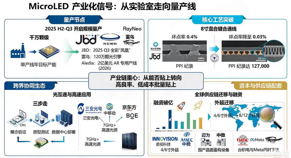
Industry Signals: From Lab to Production Line

MicroLED heterogeneous bonding is no longer confined to the laboratory. Since 2025, four signals — capacity, giants, process, and capital — all point to an industrialization window opening.

Table: Key Signals of MicroLED Industrialization

DimensionKey PlayersIndustry Signal
Mass production nodeJBD, Hongshi Intelligence, TCL RayNeoScale production begins H2–Q3 2025; single line targets annual capacity in the tens of millions of units
Core processQiushui Semiconductor, JBD, Zhejiang University8-inch hybrid bonding (HB) line in production; defect rate down to 0.03%; PPI record reaches 127,000
Cross-sector synergySan'an Optoelectronics, China Mobile, BOEDeveloped 7GHz+ high-speed light sources; CPO prototype enters validation phase
Supply chain supportNovisTech, Maxwell, AMECFinancing exceeds 100M RMB; domestic wafer restructuring equipment enables migration from 4/6-inch epitaxy to 8/12-inch silicon-based

As capacity is being built and timelines become clear, as TSMC, Meta, and other giants place bets simultaneously and the ecosystem matures, this technology is not just 'possible' but 'happening'.

The industry's focus is shifting from 'can it be bonded' to 'how to bond in volume under high-yield, low-cost conditions' — this is precisely when equipment accuracy and process stability are truly tested.

Industry Signals: From Lab to Production Line ▲ MicroLED industrialization signals: capacity, giants, process, and capital all moving toward the production window

From Process Accumulation to Equipment Deployment: Accuracy's Heterogeneous Integration Capability

In the field of heterogeneous integration, Accuracy is among the earliest domestic equipment vendors to invest in R&D and achieve real-world deployment at customer sites. In frontier directions such as nano-scale high-precision chip-to-wafer hybrid bonding, it was the first to launch joint process-equipment development with benchmark customers, accumulating deep engineering capability in thermal management, yield control, and process migration.

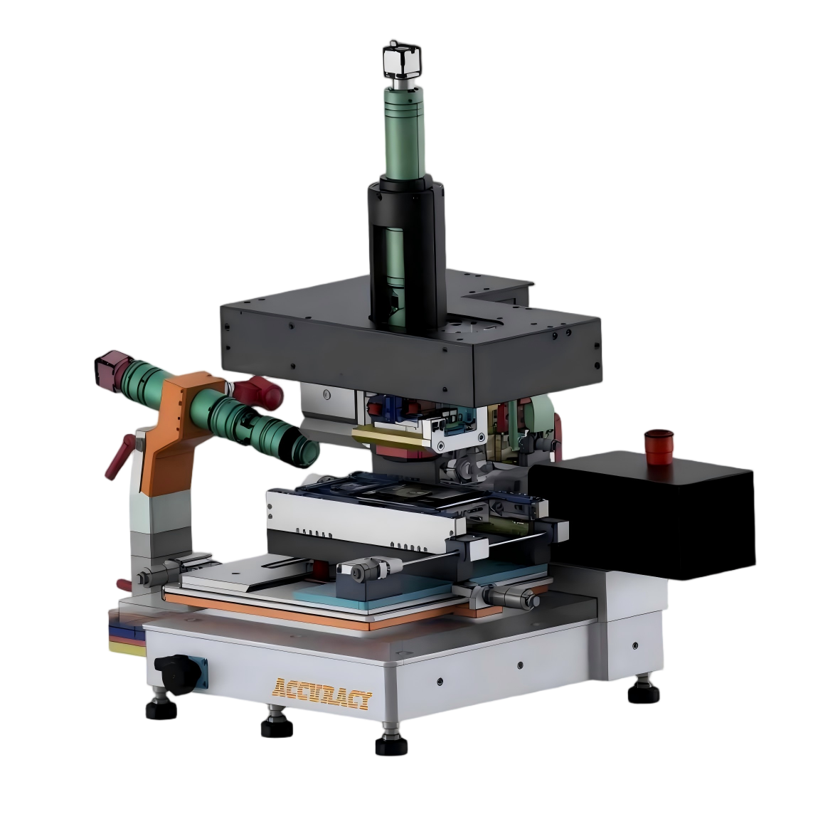
Accuracy's latest QX5000 multi-purpose sub-micron die bonder supports heterogeneous integration — enabling process development and validation for soldering, eutectic bonding, and flip-chip integration across multiple processes and material systems (GaN-on-Si / sapphire / SiC, etc.), supporting process evaluation and parameter iteration.

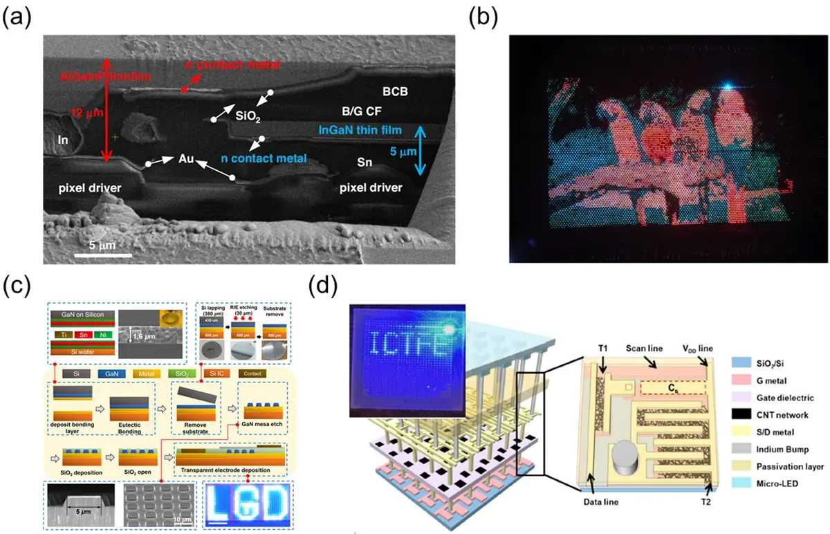
From Process Accumulation to Equipment Deployment: Accuracy's Heterogeneous Integration Capability ▲ Application case of MicroLED heterogeneous bonding using soldering and eutectic bonding [4]:
(a) Cross-sectional SEM of AlGaInP/InGaN thin films integrated with CMOS backplane via Au-In/Au-Sn soldering;
(b) 0.55-inch full-color microdisplay formed after sequential RGB MicroLED soldering;
(c) 5μm-scale GaN MicroLED array fabricated on CMOS backplane based on wafer-level eutectic bonding;
(d) InGaN MicroLED interconnected with carbon nanotube active-matrix backplane via flip-chip eutectic bonding.

Accuracy: Process Validation Services

For MicroLED heterogeneous bonding process development scenarios, the Qixin QX5000 series provides the following support:

Table: QX5000 Validation Capabilities for MicroLED Heterogeneous Bonding

Development ItemDescription
Flip-chip accuracy validation±0.5μm alignment accuracy, CPK≥1.67, meeting sub-10μm pixel pitch requirements
Multi-process route testingThermocompression (200–400°C) / cold compression (room temp), supporting parallel comparison evaluation
Force curve optimization0.1–30N full-range programming, adapting to different pad sizes and materials
Substrate compatibility evaluationGaN-on-Si / sapphire / SiC multi-scheme comparison testing
On-site process testingQX5000 prototype in Suzhou cleanroom available for booking, process team provides full support

The process route for MicroLED heterogeneous bonding is still evolving rapidly. Whether you are at the process selection evaluation, feasibility validation, or small-batch trial production stage, Accuracy has a cleanroom process validation center in Suzhou equipped with QX5000 prototypes, providing comprehensive support from process recommendations, scheme evaluation, and tool customization — offering engineering support from process design to validation deployment.

If you are evaluating MicroLED heterogeneous bonding processes, we welcome sample process trials and on-site equipment demonstrations. Book a Trial →

±0.5μm Standard-die Placement Accuracy Flip / Back Multi-Process Platform 0.1–30N Force Control Suzhou Cleanroom Validation Center

The data above reflects results from a specific project. Actual performance varies with product dimensions, material systems, process routes, and throughput (tact time); please rely on sample evaluation for confirmation.

艾科瑞思

Suzhou Accuracy Intelligent Equipment Co., Ltd., founded in 2010 and headquartered in Suzhou Industrial Park, is a professional supplier of high-precision advanced semiconductor packaging equipment, dedicated to the R&D, design, manufacture, and sale of high-accuracy, high-throughput, high-reliability, and intelligent die bonding systems.

For frontier processes such as MicroLED heterogeneous bonding, leveraging over a decade of sub-micron placement expertise, Accuracy provides customers with full-chain engineering support — from process scheme design and equipment selection to validation deployment.

References
  • [1]Ying Jiu. Academician Mao Junfa: Status and Challenges of Semiconductor Heterogeneous Integrated Circuits[J]. Electronic Engineering & Product World, 2021(8): 1-2.
  • [2]Zhang L, Ou Q, Chen S, et al. Heterogeneous Integration Technologies for Micro-LED Displays: A Review[J]. IEEE Transactions on Electron Devices, 2024.
  • [3]Yole Intelligence. MicroLED 2022 Report[R]. 2022.
  • [4]Qi Y, et al. Monolithic full-color micro-LED displays using InGaN/AlGaInP Micro-LEDs bonded on Si CMOS backplane[J]. Nature Communications, 2023.